

Fairchild Semiconductor 74ALVC16721 Datasheet
74ALVC16721
Low Voltage 20-Bit D-Type Flip-Flops
with 3.6V Tolerant Inputs and Outputs
74ALVC16721 Low Voltage 20-Bit D-Type Flip-Flops with 3.6V Tolerant Inputs and Outputs
October 2001
Revised October 2001
General Description
The ALVC16721 contains twenty non-inverting D-type
flip-flops with 3-STATE outputs and is intended for bus oriented applications.
The 74ALVC16721 is designed for low voltage (1.65V to
3.6V) V
The 74ALVC16721 is fabricated w ith an advanc ed CMOS
technology to achieve high speed operation while maintaining low CMOS power dissipation.
applications with I/O compatibility up to 3.6V.
CC
Features
■ 1.8V–3.6V VCC supply operation
■ 3.6V tolerant inputs and outputs
(CLK to On)
■ t
PD
4.0 ns max for 3.0V to 3.6V V
4.9 ns max for 2.3V to 2.7V V
8.8 ns max for 1.65V to 1.95V V
■ Power-off high impedance inputs and outputs
■ Supports live insertion and withdrawal (Note 1)
■ Uses patented noise/EMI reductio n circuitr y
■ Latchup conforms to JEDEC JED78
■ ESD performance:
Human body model
Machine model
Note 1: To ensure the high-impedance state d uring power up or power
down, OE
should be tied to VCC through a pull-up r esistor; the min imum
value of the res istor is d eter mine d by the cu rre nt-sou rcin g ca pa bility of t he
driver.
> 200V
CC
CC
CC
> 2000V
Ordering Code:
Order Number Package Number Package Description
74ALVC16721MTD MTD56 56-Lead Thin Shrink Small Outline Package (TSSOP), JEDEC MO-153, 6.1mm Wide
Device also available in Tape and Reel. Specify by appending suffix letter “X” to the ordering co de.
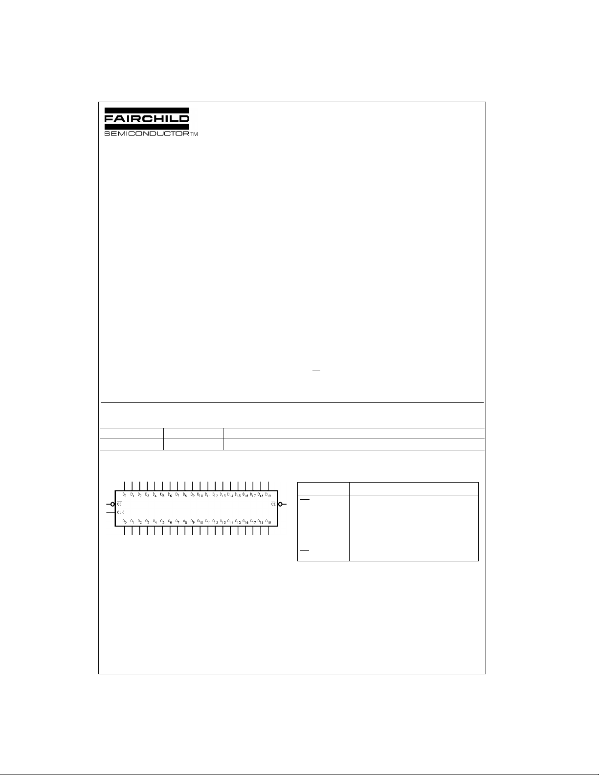
Logic Symbol Pin Descriptions
Pin Names Description
OE
CLK Clock Input
D
0–D19
O
0–O19
CE
Output Enable Input (Active LOW)
Inputs
Outputs
Clock Enable Input (Active LOW)
© 2001 Fairchild Semiconductor Corporation DS500691 www.fairchildsemi.com
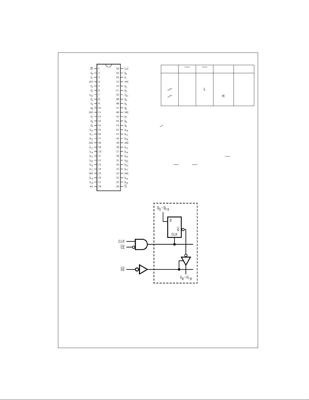
Connection Diagram Truth Table
74ALVC16721
Logic Diagram
CLK CE OE
D0–D
O0–O
19
19
XXH X Z
XHL X O
LL L L
LL H H
L or H L L X O
H = HIGH Voltage Level
L = LOW Voltage Level
X = Immaterial (HIGH or LOW, inputs may not float)
Z = High Impedance
O0 = Previous O0 before L O W-to-HIGH tran sition of Clock
= LOW-to-HIGH transition
0
0
Functional Description
The 74ALVC16721 contains twenty D-type flip-fl ops with
3-STATE standard outputs. The twenty flip-flops will store
the state of their individual D-type inputs that meet the
setup and hold time requirements on the LOW-HIGH Clock
(CLK) transition, whe n the Clock-Enable (CE
3-STATE standard outputs are controlled by the Output
Enable (OE
). When OE is HIGH , the st andard ou tputs are
in high impedance m ode but this does not interfere with
entering new data into the flip-flops.
) is LOW. The
www.fairchildsemi.com 2
 Loading...