

Fairchild Semiconductor 74AC16244 Datasheet
August 1999
Revised November 2000
74AC16244 • 74ACT16244
16-Bit Buffer/Line Driver with 3-STATE Outputs
74AC16244 • 74ACT16244 16-Bit Buffer/Line Driver with 3-STATE Outputs
General Description
The AC16244 and ACT16244 contain sixteen non-inverting
buffers with 3-STATE outputs designed to be employed as
a memory and address d river, clock driver, or bus ori ented
transmitter/receiver. The device is nibble controlled. Each
nibble has separate 3-STATE control inputs which can be
shorted together for full 16-bit operation.
Features
■ Separate control logic for each byte and nibble
■ 16-bit version of the AC244/ACT244
■ Outputs source/sink 24 mA
■ ACT16244 has TTL-compatible inputs
Ordering Code:
Order Number Package Number Package Description
74AC16244SSC MS48A 48-Lead Small Shrink Outline Package (SSOP), JEDEC MO-118, 0.300 Wide
74ACT16244SSC MS48A 48-Lead Small Shrink Outline Package (SSOP), JEDEC MO-118, 0.300 Wide
74ACT16244MTD MTD48 48-Lead Thin Shrink Small Outline Package (TSSOP), JEDEC MO-153, 6.1mm Wide
Device also available in Tape and Reel. Specify by appending suffix letter “X” to the or dering code.
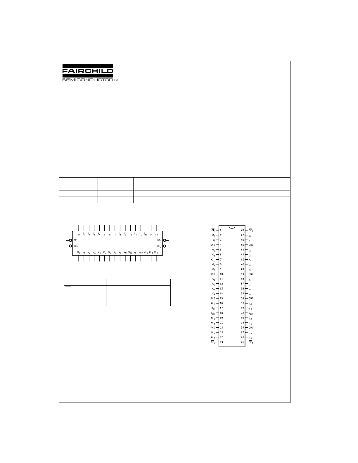
Logic Symbol
Connection Diagram
Pin Descriptions
Pin Names Description
OE
I
0
O
- I
0
n
- 0
15
15
Output Enable Input (Active LOW)
Inputs
Outputs
FACT is a trademark of Fairchild Semiconductor Corporation.
© 2000 Fairchild Semiconductor Corporation DS500295 www.fairchildsemi.com
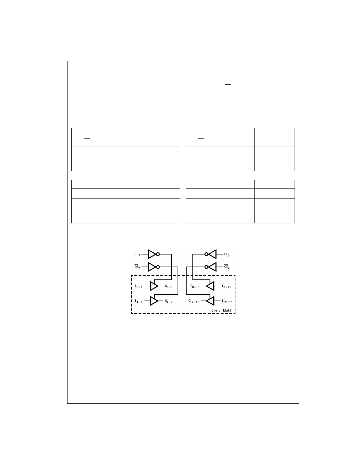
Functional Description
The AC16244 and ACT16244 contain sixteen non-inverting
buffers with 3-STATE stand ard outputs. The device is nibble (4 bits) controlle d with each nibble functioning iden tically, but independent of the othe r. The control p i ns c an b e
shorted together to obtain full 16-bit operation. The
Truth Tables
3-STATE outputs are controlled by an Output Enable (OE
input for each nibble. When OE
2-state mode. Wh en OE
is LOW, the outputs are in
n
is HIGH, the outputs are in the
n
high impedance mode, but this does not interfere with
entering new data into the inputs.
)
n
74AC16244 • 74ACT16244
OE
1
LL L
LH H
HX Z
OE
3
LL L
LH H
HX Z
L = LOW Voltage Level
H = HIGH Voltage Level
Logic Diagram
Inputs Outputs
I0–I
3
O0–O
Inputs Outputs
I8–I
11
O8–O
Inputs Outputs
3
OE
2
I4–I
7
O4–O
7
LL L
LH H
HX Z
Inputs Outputs
11
OE
4
I12–I
15
O12–O
15
LL L
LH H
HX Z
X = Immaterial
Z = High Impedance
www.fairchildsemi.com 2
Absolute Maximum Ratings(Note 1) Recommended Operating
Supply Voltage (VCC) −0.5V to +7.0V
DC Input Diode Current (I
V
= − 0.5V −20 mA
I
= VCC + 0.5V +20 mA
V
I
DC Output Diode Current (I
V
= −0.5V −20 mA
O
= VCC + 0.5V +20 mA
V
O
DC Output Voltage (V
DC Output Source/Sink Current (I
or Ground Current
DC V
CC
per Output Pin
Junction Temperature
Storage Temperature
)
IK
)
OK
) −0.5V to VCC + 0.5V
O
) ±50 mA
O
±50 mA
+140°C
−65°C to +150°C
Conditions
Supply Voltage (V
AC 2.0V to 6.0V
ACT 4.5V to 5.5V
Input Voltage (V
Output Voltage (VO)0V to V
Operating Temperature (TA) −40°C to +85°C
Minimum Input Edge Rate (
AC Devices
V
from 30% to 70%
IN
V
@ 3.3V, 4.5V, 5.5V 125 mV/ns
CC
Minimum Input Edge Rate (
ACT Devices
V
from 0.8V to 2.0V
IN
@ 4.5V, 5.5V 125 mV/ns
V
CC
Note 1: Absolute max imum ratings are those values beyond w hich damage
to the device may occu r. The databook spe cificatio ns shou ld be met, w ithout exception to ensure that the system design is reliable over its power
supply, temperature, and output/input loading variables. Fairchild does not
recommend operation of FACT circuits ou tside databook spec if ic at ions.
)
CC
)0V to V
I
∆V/∆t)
∆V/∆t)
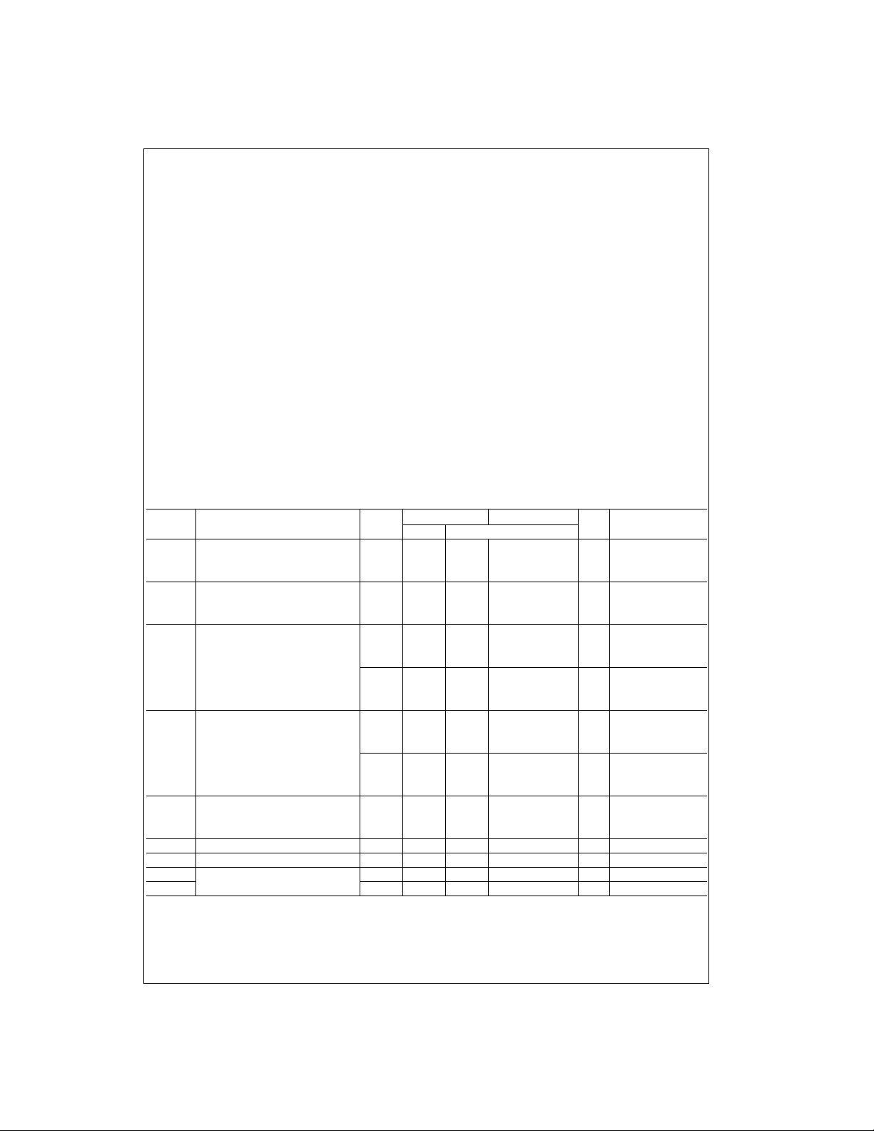
DC Electrical Characteristics for AC
V
Symbol Parameter
V
V
V
V
I
OZ
I
IN
I
CC
I
OLD
I
OHD
Note 2: All outputs loaded; thresholds associated with output under test.
Note 3: I
Note 4: Maximum test duration 2.0 millisecond; one out put loaded at a time.
Minimum HIGH Input Voltage 3.0 1.5 2.1 2.1
IH
Maximum LOW Input Voltage 3.0 1.5 0.9 0.9
IL
Minimum HIGH Output Voltage 3.0 2.99 2.9 2.9
OH
Maximum LOW Output Voltage 3.0 0.002 0.1 0.1
OL
Maximum 3-STATE Leakage Current 5.5 0.50 ± 5.0 µAVI (OE) = VIL, V
Maximum Input Leakage Current (Note 3) 5.5 ± 0.1 ± 1.0 µAVI = VCC, GND
Max Quiescent Supply Current (Note 3) 5.5 8.0 80.0 µAVIN = VCC or GND
Minimum Dynamic 5.5 75 mA V
Output Current (Note 4) 5.5 −75 mA V
and ICC @ 3.0V are guaranteed to be less than or e qual to the respective lim it @ 5. 5V VCC.
IN
CC
(V) Typ Guaranteed Limits
4.5 2.25 3.15 3.15 or VCC − 0.1V
5.5 2.75 3.85 3.85
4.5 2.25 1.35 1.35 or VCC − 0.1V
5.5 2.75 1.65 1.65
5.5 5.49 5.4 5.4
3.0 2.56 2.46 IOH = -12 mA
4.5 3.86 3.76 V IOH = −24 mA
5.5 4.86 4.76 I
5.5 0.001 0.1 0.1
3.0 0.36 0.44 IOL = 12 mA
4.5 0.36 0.44 V IOL = 24 mA
5.5 0.36 0.44 IOL = 24 mA (Note 2)
TA = +25°CTA = −40°C to +85°C
Units Conditions
V
V
VI
VI
V
= 0.1V
OUT
V
= 0.1V
OUT
= −50 µA4.5 4.49 4.4 4.4
OUT
= −24 mA (Note 2)
OH
= 50 µA4.5 0.001 0.1 0.1
OUT
VI = VCC, GND
VO = VCC, GND
= 1.65V Max
OLD
= 3.85V Min
OHD
74AC16244 • 74ACT16244
CC
CC
IH
3 www.fairchildsemi.com
 Loading...