Fairchild TN6729A, NZT6729 service manual

TN6729A / NZT6729
TN6729A
C
B
E
TO-226
NZT6729
C
E
C
B
SOT-223
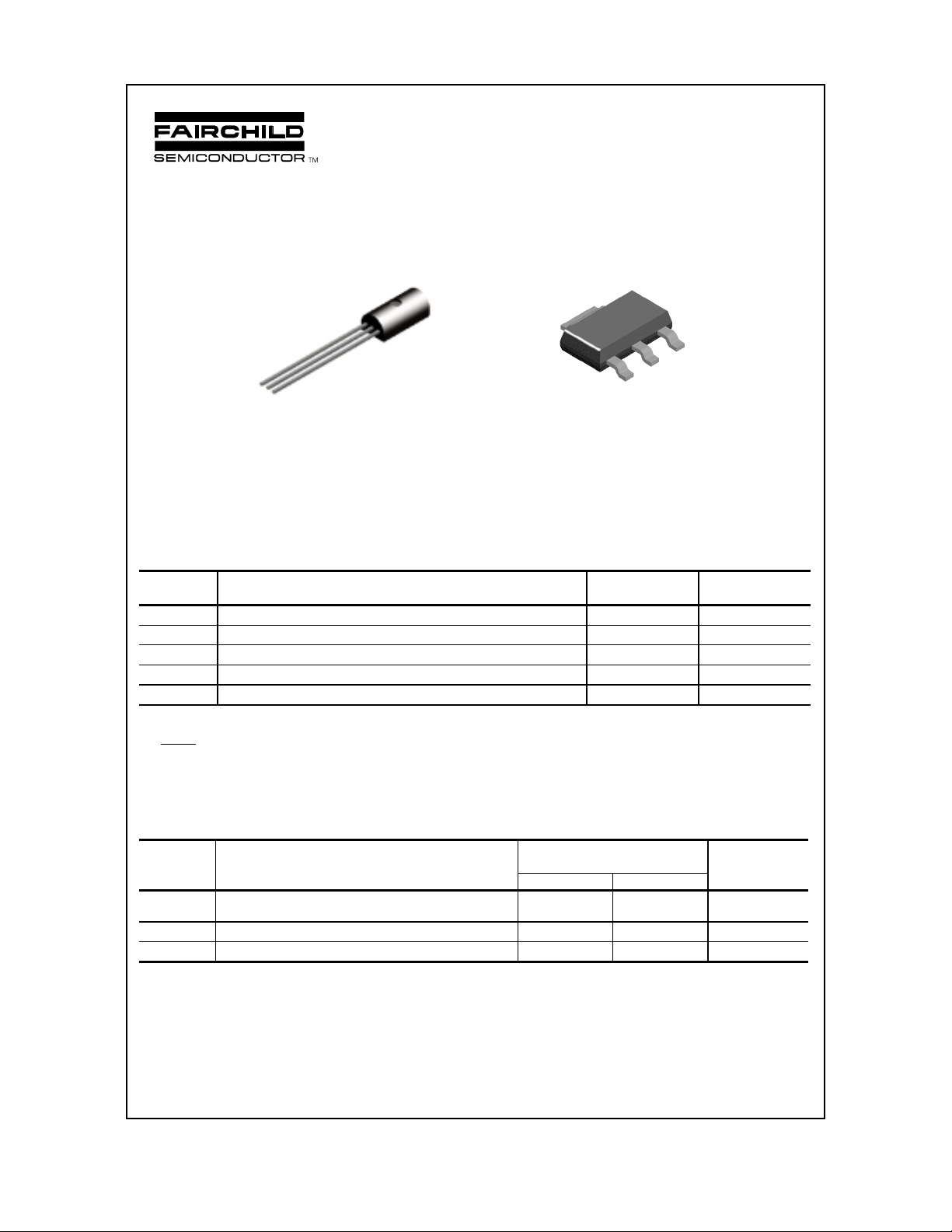
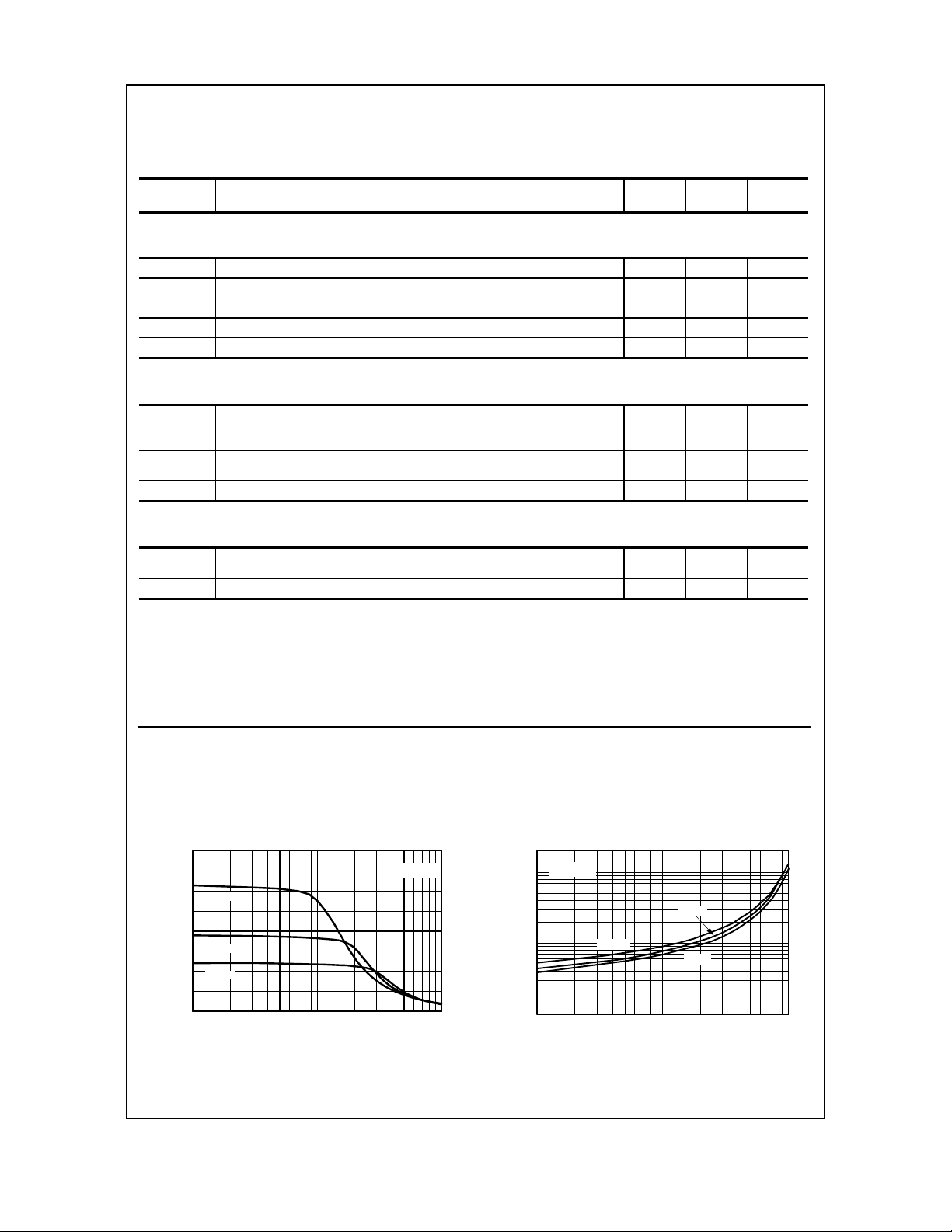
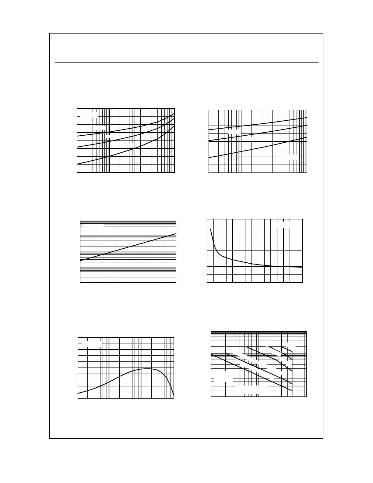
PNP General Purpose Amplifier
This device is designed for general purpose medium power
amplifiers and switches requiring collector currents to 800
mA. Sourced from Process 79.
Absolute Maximum Ratings* TA = 25°C unless otherwise noted
Symbol Parameter Value Units
V
CEO
V
CBO
V
EBO
I
C
TJ, T
stg
*These ratings are limiting values above which the serviceability of any semiconductor device may be impaired.
NOTES:
1) These ratings are based on a maximum junction temperature of 150 degrees C.
2) These are steady state limits. The factory should be consulted on applications involving pulsed or low duty cycle operations.
3) All voltages (V) and currents (A) are negative polarity for PNP transistors.
Collector-Emitter Voltage 80 V
Collector-Base Voltage 80 V
Emitter-Base Voltage 5.0 V
Collector Current - Continuous 1.0 A
Operating and Storage Junction Temperature Range -55 to +150
C
°
Thermal Characteristics TA = 25°C unless otherwise noted
Symbol Characteristic Max Units
TN6729A *NZT6729
P
D
R
θ
JC
R
θ
JA
*Device mounted on FR-4 PCB 36 mm X 18 mm X 1.5 mm; mounting pad for the collector lead min. 6 cm
1997 Fairchild Semiconductor Corporation
Total Devi ce Dissipat ion
Derate above 25°C
Thermal Resistance, Junction to Case 50
Thermal Resistance, Junction to Ambient 125 125
1.0
8.0
1.0
8.0
2
.
W
mW/°C
C/W
°
C/W
°

µ
µ
PNP General Purpose Amplifier
(continued)
Electrical Characteristics TA = 25°C unless otherwise noted
Symbol Parameter Test Conditions Min Max Units
OFF CHARACTERISTICS
V
(BR)CEO
V
(BR)CBO
V
(BR)EBO
I
CBO
I
EBO
ON CHARACTERISTICS*
h
FE
V
sat
CE(
V
BE(on)
Collector-Emitter Breakdown Voltage IC = 1.0 mA, IB = 0 80 V
Collector-Base Breakdown Voltage
I
= 100 µA, IE = 0
C
80 V
Emitter-Base Breakdown Voltage IE = 1.0 mA, IC = 0 5.0 V
Collector-Cutoff Current VCB = 60 V, IE = 0 0.1
Emitte r-Cutoff Current VEB = 5.0 V, IC = 0 10
DC Current Gain IC = 50 mA, VCE = 1.0 V
I
= 250 mA, VCE = 1.0 V
C
I
= 500 mA, VCE = 1.0 V
Collector-Emitter Saturation Voltage IC = 250 mA, IB = 10 mA
)
C
= 250 mA, IB = 25 mA
I
C
80
50
20
Base-Emitter On Vol t age IC = 250 mA, VCE = 1.0 V 1.2 V
250
0.5
0.35
A
A
V
V
TN6729A / NZT6729
SMALL SIGNAL CHARACTERISTICS
h
fe
C
cb
Small-Signal Current Gain IC = 200 mA, VCE = 5.0 V,
f = 20 MHz
Collector-Base Capacitance VCB = 10 V, IE = 0, f = 1.0 MHz 30 pF
*Pulse T est: Pulse Width ≤ 300 µs, Duty Cycle ≤ 1.0%
NOTE: All voltages (V) and currents (A) are negative polarity for PNP transistors.
T ypical Characteristics
Typical Pulsed Current Gain
vs Collector Current
200
V = 1.0 V
CE
150
125 °C
100
25 °C
50
- 40 °C
2.5 25
Co llecto r-Emitt er Sa turatio n
Volt a ge v s C ollec t or Current
2
= 10
β
1
0.1
- 40 °C
3
25 °C
125 °C
0
FE
0.01 0.02 0.05 0.1 0.5 1
h - TYPICAL PULSED CURRENT GAIN
I - COLLECTOR CURRENT (A)
C
0.01
10 10 0 1000
CE SAT
V - COL LEC TOR EMI TTER VOL TAGE (V)
I - COLLECTOR CURRENT (mA)
C

Typical Characteristics (continued)
TN6729A / NZT6729
PNP General Purpose Amplifier
(continued)
Base-Em itter Sa turati o n
Voltag e vs Coll ector Cur re nt
β
= 10
1
0.8
0.6
- 40 °C
25 °C
125 °C
0.4
BE SAT
V - BASE EMITTER VOLTAGE (V)
1 10 100 1000
I - COLLECTOR CURRE NT (mA)
C
Collect or-Cutoff Current
vs Amb ie nt Temp eratu re
100
V = 60V
CB
10
1
0.1
Base Emitter ON Voltage vs
Collector Current
1
0.8
- 40 °C
0.6
0.4
0.2
BE(ON)
1 10 100 1000
V - BASE EMITTER ON VOL TAGE (V)
I - COLLECTOR CURRE NT (mA)
C
25 °C
125 °C
V = 5V
CE
Collector-Base Capacitance
vs Collector-Base Voltage
40
30
20
10
f = 1.0 MHz
CBO
I - C OLLE CT OR CU RREN T (nA)
0.01
25 50 75 100 125
T - AM BI E NT TEM P E R ATU R E ( C)
A
°
Gain Bandwidth Product
vs Collector Current
250
V = 10V
CE
200
150
100
50
0
T
1 10 100 1000
f - GAIN BANDWIDTH PRODUCT (MHz)
I - COL LECTOR CURRENT (mA)
C
0
0 4 8 12 16 20 24 28
obo
V - COL L ECTOR -BAS E VOLTAGE (V )
- COLLE CTO R- BA SE CAPACITANCE (pF)
CB
Safe O perating Area TO-226 / SOT- 223
10
10
µ
1
*PULSED
0.1
OPERATION
T = 25 °C
A
C
I - COLLE CTOR CURRENT (A)
0.01
1 10 100
DC T = 25 °C
COLLECTOR LEAD
DC T = 25 °C
AMBIENT
LIMIT DETERMINED
BY BV
V - COLLECTOR -EMITTER VOLTAGE (V)
CE
100
CEO
S*
µ
S*
1.0 ms*

Typical Characteristics (continued)
Power Dissipati on vs
Ambient Temperature
1
TN6729A / NZT6729
PNP General Purpose Amplifier
(continued)
0.75
0.5
0.25
D
P - P OWER DISSIPATION (W)
0
0 25 50 75 100 125 150
TO-226
SOT-223
TEMPERATURE ( C)
o
3
 Loading...