Fairchild NDS8852H service manual

查询NDS8852H供应商
NDS8852H
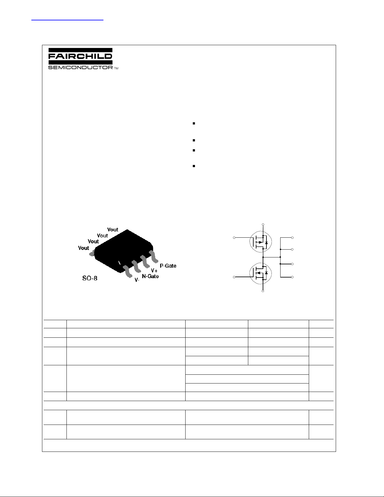
Complementary MOSFET Half Bridge
General Description Features
February 1996
These Complementary MOSFET half bridge devices are
produced using Fairchild's proprietary, high cell density,
DMOS technology. This very high density process is
especially tailored to minimize on-state resistance, provide
superior switching performance, and withstand high energy
pulses in the avalanche and commutation modes. These
devices are particularly suited for low voltage half bridge
applications or CMOS applications when both gates are
connected together.
N-Channel 4.3A, 30V, R
P-Channel -3.4A, -30V, R
High density cell design or extremely low R
=0.08Ω @ V
DS(ON)
DS(ON)
=0.13Ω @ V
GS
GS
DS(ON)
=10V.
=-10V.
.
High power and current handling capability in a widely used
surface mount package.
Matched pair for equal input capacitance and power capability
.
________________________________________________________________________________
V+
P-Gate
N-Gate
V-
Vout
Vout
Vout
Vout
Absolute Maximum Ratings T
= 25°C unless otherwise noted
A
Symbol Parameter N-Channel P-Channel Units
V
DSS
V
GSS
I
D
Drain-Source Voltage 30 -30 V
Gate-Source Voltage 20 -20 V
Drain Current - Continuous (Note 1a & 2) 4.3 -3.4 A
- Pulsed 15 -10
P
D
Maximum Power Dissipation (Note 1a) 2.5 W
(Single Device) (Note 1b) 1.2
(Note 1c) 1
TJ,T
Operating and Storage Temperature Range -55 to 150 °C
STG
THERMAL CHARACTERISTICS
R
θ
R
θ
© 1997 Fairchild Semiconductor Corporation
Thermal Resistance, Junction-to-Ambient
JA
(Single Device) (Note 1a)
Thermal Resistance, Junction-to-Case
JC
(Single Device) (Note 1)
50 °C/W
25 °C/W
NDS8852H Rev. C1

Electrical Characteristics (T
= 25°C unless otherwise noted)
A
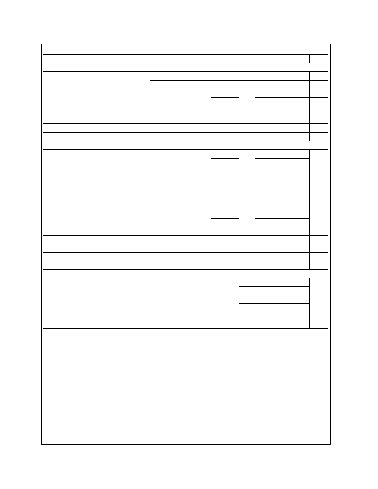
Symbol Parameter Conditions Type Min Typ Max Units
OFF CHARACTERISTICS
BV
I
DSS
I
GSSF
I
GSSR
DSS
Drain-Source Breakdown Voltage VGS = 0 V, ID = 250 µA N-Ch 30 V
VGS = 0 V, ID = -250 µA
Zero Gate Voltage Drain Current VDS = 24 V, V
VDS = -24 V, V
= 0 V N-Ch 2 µA
GS
TJ = 55oC
= 0 V P-Ch -2 µA
GS
TJ = 55oC
P-Ch -30 V
25 µA
-25 µA
Gate - Body Leakage, Forward VGS = 20 V, VDS = 0 V All 100 nA
Gate - Body Leakage, Reverse
VGS = -20 V, VDS= 0 V
All -100 nA
ON CHARACTERISTICS (Note 3)
V
R
GS(th)
DS(ON)
Gate Threshold Voltage
Static Drain-Source On-Resistance
VDS = VGS, ID = 250 µA
TJ = 125oC
VDS = VGS, ID = -250 µA
TJ = 125oC
VGS = 10 V, ID = 3.4 A
N-Ch 1 1.7 2.8 V
0.7 1.2 2.2
P-Ch -1 -1.6 -2.8
-0.85 -1.25 -2.5
N-Ch 0.06 0.08
TJ = 125oC 0.08 0.13
VGS = 4.5 V, ID = 2.8 A
0.08 0.11
VGS = -10 V, ID = -3.4 A P-Ch 0.11 0.13
TJ = 125oC
0.15 0.21
VGS = -4.5 V, ID = -2.8 A 0.17 0.2
I
D(on)
On-State Drain Current
VGS = 10 V, VDS = 5 V
N-Ch 10 A
VGS = -10 V, VDS = -5 V P-Ch -10
g
FS
Forward Transconductance
VDS = 15 V, ID = 3.4 A
N-Ch 6 S
VDS = -15 V, ID = -3.4 A P-Ch 4
DYNAMIC CHARACTERISTICS
C
iss
Input Capacitance N-Channel
VDS = 15 V, VGS = 0 V,
f = 1.0 MHz
C
oss
C
rss
Output Capacitance N-Ch 190 pF
P-Channel
Reverse Transfer Capacitance N-Ch 70 pF
VDS = -15 V, VGS = 0 V,
f = 1.0 MHz
N-Ch 300 pF
P-Ch 330
P-Ch 190
P-Ch 70
Ω
NDS8852H Rev. C1

Electrical Characteristics (T
= 25°C unless otherwise noted)
A
Symbol Parameter Conditions Type Min Typ Max Units
SWITCHING CHARACTERISTICS (Note 3)
t
t
t
t
D(on)
r
D(off)
f
Turn - On Delay Time N-Channel
VDD = 10 V, ID = 1 A,
V
= 10 V, R
Turn - On Rise Time N-Ch 13 20 ns
GEN
GEN
= 6 Ω
P-Channel
Turn - Off Delay Time N-Ch 21 50 ns
VDD = -10 V, ID = -1 A,
V
= -10 V, R
GEN
GEN
= 6 Ω
N-Ch 10 15 ns
P-Ch 9 40
P-Ch 21 40
P-Ch 21 90
Turn - Off Fall Time N-Ch 5 50 ns
P-Ch 8 50
Q
g
Q
gs
Q
gd
Total Gate Charge N-Channel
VDS = 10 V,
ID = 3.4 A, VGS = 10 V
Gate-Source Charge N-Ch 1.5
P-Channel
VDS = -10 V,
Gate-Drain Charge N-Ch 2.6
ID = -3.4 A, VGS = -10 V
N-Ch 9.5 27 nC
P-Ch 10 25
P-Ch 1.6
P-Ch 2.7
DRAIN-SOURCE DIODE CHARACTERISTICS AND MAXIMUM RATINGS
I
S
Maximum Continuous Drain-Source Diode Forward Current N-Ch 2.1 A
P-Ch -2.1
V
SD
t
rr
Drain-Source Diode Forward
Voltage
VGS = 0 V, IS = 2.1 A
VGS = 0 V, IS = -2.1 A
Reverse Recovery Time N-Channel
VGS = 0 V, IF = 2.1 A, dIF/dt = 100 A/µs
P-Channel
(Note 2) N-Ch 0.8 1.2 V
(Note 2)
P-Ch -0.8 -1.2
N-Ch 100 ns
P-Ch 100
VGS = 0 V, IF = -2.1 A, dIF/dt = 100 A/µs
Notes:
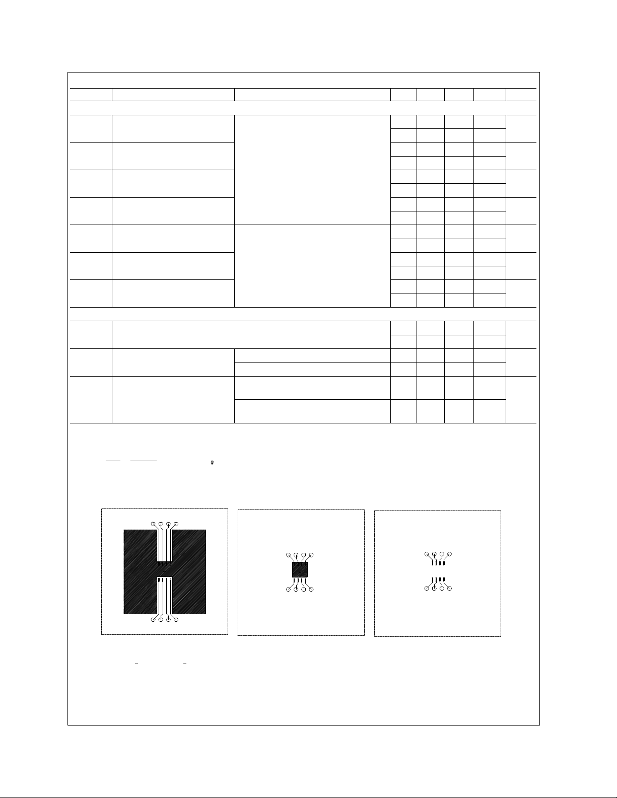
1. R
is the sum of the junction-to-case and case-to-ambient thermal resistance where the case thermal reference is defined as the solder mounting surface of the drain pins. R
JA
θ
design while R
(t)
P
D
Typical R
is determined by the user's board design.
CA
θ
T
−T
T
J
=
R
θJ A
using the board layouts shown below on 4.5"x5" FR-4 PCB in a still air environment:
JA
θ
a. 50oC/W when mounted on a 1 in2 pad of 2oz cpper.
b. 105oC/W when mounted on a 0.04 in2 pad of 2oz cpper.
c. 125oC/W when mounted on a 0.006 in2 pad of 2oz cpper.
1a
−T
J
A
(t)
A
=
R
θ
J C
2
= I
(t) × R
DS (ON ) T
D
+R
(t)
θ
CA
J
1b
1c
is guaranteed by
JC
θ
Scale 1 : 1 on letter size paper
2. Pulse Test: Pulse Width < 300µs, Duty Cycle < 2.0%.
NDS8852H Rev. C1

Typical Electrical Characteristics
20
15
10
5
D
I , DRAIN-SOURCE CURRENT (A)
0
0 1 2 3
V =10V
GS
8.0
6.0
5.0
V , DRAIN-SOURCE VOLTAGE (V)
DS
4.5
4.0
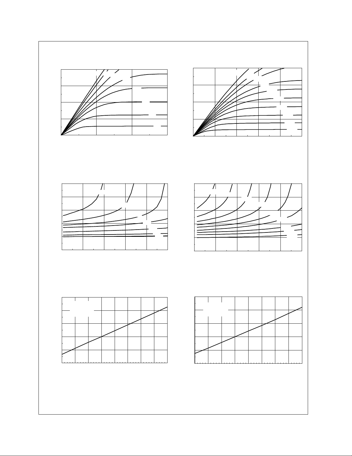
Figure 1. N-Channel On-Region Characteristics.
3
V = 3.5V
2.5
GS
4.0
2
1.5
DS(on)
R , NORMALIZED
1
DRAIN-SOURCE ON-RESISTANCE
0.5
0 3 6 9 12 15
I , DRAIN CURRENT (A)
D
4.5
5.0
Figure 3. N-Channel On-Resistance Variation with
Gate Voltage and Drain Current.
3.5
6.0
3.0
8.0
10
-20
-15
V = -10V
GS
-8.0
-7.0
-6.0
-5.5
-10
-5
D
I , DRAIN-SOURCE CURRENT (A)
0
V , DRAIN-SOURCE VOLTAGE (V)
DS
-5.0
Figure 2. P-Channel On-Region Characteristics.
3
V = -3.5V
2.5
GS
-4.0
-4.5
-5.0
2
1.5
DS(on)
R , NORMALIZED
1
DRAIN-SOURCE ON-RESISTANCE
0.5
I , DRAIN CURRENT (A)
D
-5.5
Figure 4. P-Channel On-Resistance Variation
with Gate Voltage and Drain Current.
-4.5
-6.0
-4.0
-7.0
-8.0
-3.5
-3.0
-5-4-3-2-10
-10
-15-12-9-6-30
1.6
I = 3.4A
1.4
1.2
DS(ON)
R , NORMALIZED
0.8
DRAIN-SOURCE ON-RESISTANCE
0.6
D
V = 10V
GS
1
-50 -25 0 25 50 75 100 125 150
T , JUNCTION TEMPERATURE (°C)
J
Figure 5. N-Channel On-Resistance Variation
with Temperature.
1.6
I = -3.4A
1.4
1.2
DS(ON)
R , NORMALIZED
0.8
DRAIN-SOURCE ON-RESISTANCE
0.6
D
V = -10V
GS
1
-50 -25 0 25 50 75 100 125 150
T , JUNCTION TEMPERATURE (°C)
J
Figure 6. P-Channel On-Resistance Variation
with Temperature.
NDS8852H Rev. C1
 Loading...