

Fairchild NC7SZ02 service manual
NC7SZ02
NC7SZ02 TinyLogic
October 1996
Revised June 2000
TinyLogic
General Description
The NC7SZ02 is a single 2-Input NOR Gate from Fairchild’s Ultra High Speed Series of TinyLogic
is fabricated with a dvanced CMOS technolo gy to achieve
ultra high speed with high outpu t drive while maintaining
low static power dissipa tion over a very b road V
ing range. The device is specified to operate ove r the 1.8V
to 5.5V V
CC
ance when V
independent of V
UHS 2-Input NOR Gate
. The device
operat-
CC
range. The inputs an d output ar e high im ped-
is 0V. Inputs tolerate voltages up to 6V
CC
operating voltage.
CC
Features
■ Space saving SOT23 or SC70 5-lead package
■ Ultra High Speed: t
■ High Output Drive: ±24 mA at 3V V
■ Broad VCC Operating Range: 1.8V–5.5V
■ Matches the performance of LCX when operated at
3.3V V
CC
■ Power down high impedance inputs/output
■ Overvoltage tolerant inputs facilitate 5V to 3V
translation
■ Patented noise/EMI reduction circuitry implemented
2.4 ns typ into 50 pF at 5V V
PD
CC
CC
Ordering Code:
Order Package Product Code
Number Number Top Mark
NC7SZ02M5 MA05B 7Z02 5-Lead SOT23, JEDEC MO-178, 1.6mm 250 Units on Tape and Reel
NC7SZ02M5X MA05B 7Z02 5-Lead SOT23, JEDEC MO-178, 1.6mm 3k Units on Tape and Reel
NC7SZ02P5 MAA05A Z02 5-Lead SC70, EIAJ SC-88a, 1.25mm Wide 250 Units on Tape and Reel
NC7SZ02P5X MAA05A Z02 5-Lead SC70, EIAJ SC-88a, 1.25mm Wide 3k Units on Tape and Reel
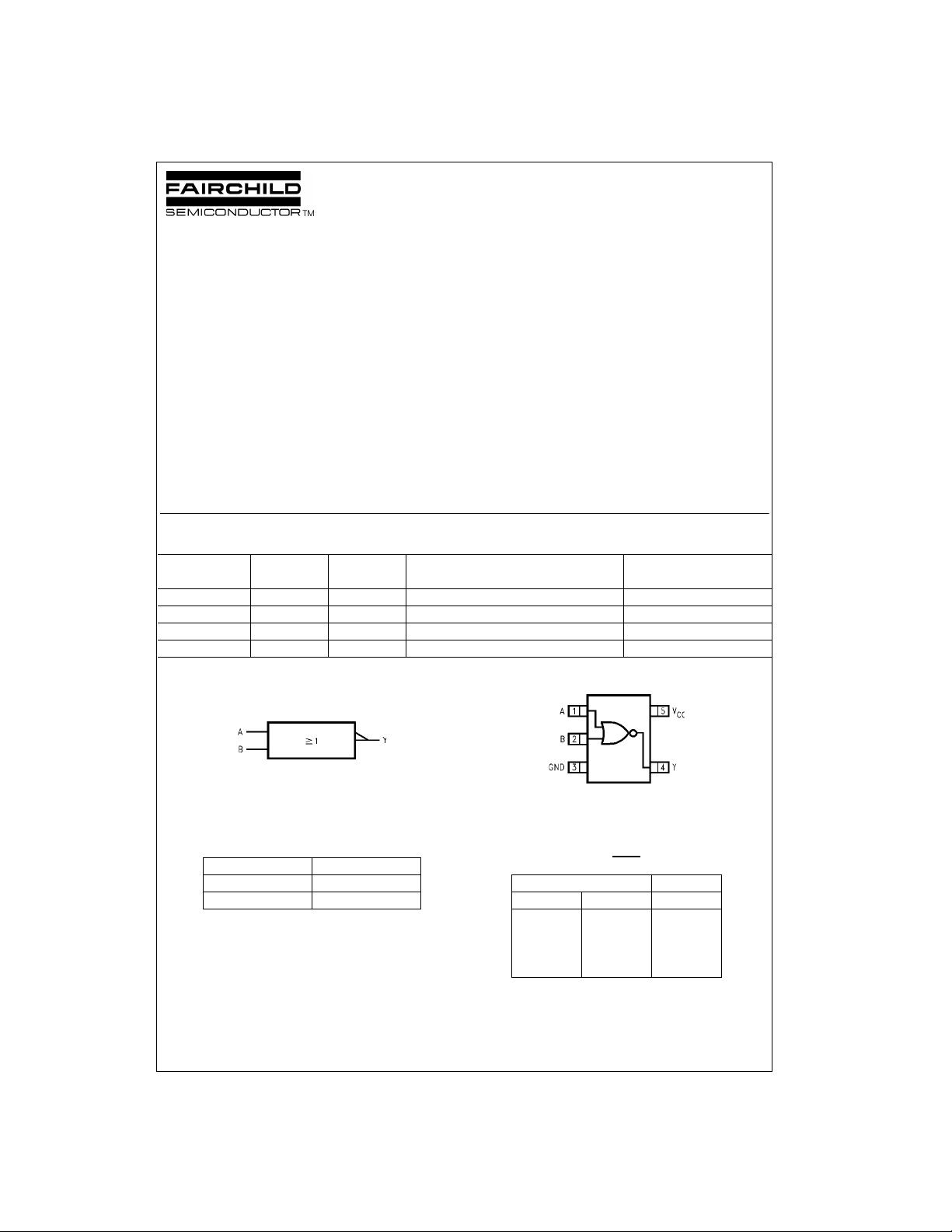
Logic Symbol
IEEE/IEC
Package Descript ion Supplied As
Connection Diagram
UHS 2-Input NOR Gate
(Top View)
Pin Descriptions Function Table
Pin Names Description
A, B Inputs
Y Output
H = HIGH Logic Level
L = LOW Logic Level
TinyLogic is a trademark of Fairchild Semiconductor Co rporation.
© 2000 Fairchild Semiconductor Corporation DS012167 www.fairchildsemi.com
ABY
LLH
LHL
HLL
HHL
Y = A + B
Inputs Output
Absolute Maximum Ratings(Note 1) Recommended Operating
Supply Voltage (VCC) −0.5V to +6V
DC Input Voltage (V
NC7SZ02
DC Output Voltage (V
DC Input Diode Current (I
@ V
< −0.5V −50 mA
IN
@ V
> 6V +20 mA
IN
DC Output Diode Current (I
@ V
< −0.5V −50 mA
OUT
@ V
> 6V, VCC = GND +20 mA
OUT
DC Output Current (I
DC V
/GND Current (ICC/I
CC
Storage Temperature (T
Junction Temperature under Bias (T
Junction Lead Temperature (T
) −0.5V to +6V
IN
) −0.5V to +6V
OUT
)
IK
)
OK
) ± 50 mA
OUT
) ± 50 mA
GND
) −65°C to +150°C
STG
) 150°C
J
);
L
(Soldering, 10 seconds) 260
Power Dissipation (P
) @ +85°C
D
SOT23-5 200 mW
SC70-5 150 mW
Conditions
Supply Voltage Operating (V
Supply Voltage Data Retention (V
Input Voltage (V
Output Voltage (V
Operating Temperature (TA) −40°C to +85°C
Input Rise and Fall Time (t
@ 1.8V, 2.5V ±0.2V 0 ns/V to 20 ns/V
V
CC
V
@ 3.3V ± 0.3V 0 ns/V to 10 ns/V
CC
V
@ 5.0V ± 0.5V 0 ns to 5 ns/V
CC
Thermal Resistance (
SOT23-5 300
SC70-5 425
Note 1: Absolute maximum ratings are DC values beyond which the devi ce
°C
may be damage d or h ave its us eful life im pai red. Th e dat as heet sp ecific ations should be met, without exception, to ensure that the system design is
reliable over its power supply, temperature, and output/input loading variables. Fairchild does no t recommend operation outsid e datasheet spec ifications.
Note 2: Unused inputs must be held HIGH or LOW. They may not float.
(Note 2)
) 1.8V to 5.5V
CC
)0V to 5.5V
IN
) 0V to V
OUT
, tf)
r
θ
)
JA
DC Electrical Characteristics
Symbol Parameter
V
V
V
V
I
I
I
HIGH Level Input Voltage 1.8 0.75V
IH
LOW Level Input Voltage 1.8 0.25V
IL
HIGH Level Output Voltage 1.8 1.7 1.8 1.7
OH
LOW Level Output Voltage 1.8 0.0 0.1 0.1
OL
Input Leakage Current 0-5.5 ±1 ±10 µAVIN = 5.5V, GND
IN
Power Off Leakage Current 0.0 1 10 µAVIN or V
OFF
Quiescent Supply Current 1.8-5.5 2.0 20 µAVIN = 5.5V, GND
CC
V
CC
(V) Min Typ Max Min Max
2.3–5.5 0.7 V
2.3–5.5 0.3 V
2.3 2.2 2.3 2.2
3.0 2.9 3.0 2.9
4.5 4.4 4.5 4.4
2.3 1.9 2.15 1.9
3.0 2.4 2.80 2.4 I
3.0 2.3 2.68 2.3 I
4.5 3.8 4.20 3.8 IOH=−32mA
2.3 0.0 0.1 0.1
3.0 0.0 0.1 0.1
4.5 0.0 0.1 0.1
2.3 0.10 0.3 0.3
3.0 0.15 0.4 0.4 IOL=16mA
3.0 0.22 0.55 0.55 IOL=24mA
4.5 0.22 0.55 0.55 IOL=32mA
TA = +25°CT
CC
CC
A
0.75V
0.7 V
CC
CC
= −40°C to +85°C
CC
CC
0.25V
CC
0.3 V
CC
Units Conditions
) 1.5V to 5.5V
CC
CC
°C/W
°C/W
V
V
VVIN = VILIOH=−100µA
IOH=−8mA
=−16mA
OUT
OH
=−24mA
OH
IOL= 8mA
= 5.5V
V
VVIN=VIHIOL=100µA
V
www.fairchildsemi.com 2
AC Electrical Characteristics
V
Symbol Parameter
t
, Propagation Delay 1.8 2.0 4.4 9.5 2.0 10
PLH
t
PHL
CC
(V) Min Typ Max Min Max
2.5 ± 0.2 0.8 2.9 6.5 0.8 7.0 CL = 15 pF,
3.3 ± 0.3 0.5 2.3 4.5 0.5 4.7 R
5.0 ± 0.5 0.5 1.9 3.9 0.5 4.1
Propagation Delay 3.3 ± 0.3 1.5 2.9 5.0 1.5 5.2
t
PLH,
t
PHL
Input Capacitance 0 4 pF
C
IN
C
Power Dissipation 3.3 23
PD
5.0 ± 0.5 0.8 2.4 4.3 0.8 4.5 RL = 500Ω
Capacitance 5.0 30
Note 3: CPD is defined as the value of the internal equivalent capacitance which is derived from dynamic operating current consumption (I
loading and operating at 50% duty cycle. (See Figure 2.) C
= (CPD)(VCC)(fIN) + (ICCstatic).
I
CCD
TA = +25°CT
is related to I
PD
dynamic operating current by the express ion:
CCD
= −40°C to +85°C
A
Units Conditions Fig. No.
ns
= 1 MΩ
L
CL = 50 pF,
ns
pF (Note 3) Figure 2
AC Loading and Waveforms
CL includes load and s tr ay c apacitance
Input PR R = 1.0 MHz; t
= 500 ns
w
FIGURE 1. AC Test Circuit
) at no output
CCD
Figures
1, 3
Figures
1, 3
NC7SZ02
Input = AC Wavefor m; tr = tf = 1.8 ns;
PRR = 10 MHz; Duty Cycle = 50%
FIGURE 2. I
Test Circuit
CCD
FIGURE 3. AC Waveforms
3 www.fairchildsemi.com
 Loading...