

NC7SV14
NC7SV14 TinyLogic
June 2001
Revised March 2004
TinyLogic
ULP-A Inverter with Schmitt Trigger Input
General Description
The NC7SV14 is a single inverter with Schmitt trigger from
Fairchild’s Ultra Low Power-A (ULP-A) Series of
TinyLogic
. ULP-A is ideal for applications that require
extreme high speed, high drive and low po wer. This product is designed for a wide low voltage operating range
(0.9V to 3.6V V
and speed than the TinyLogic ULP series, but still offer
best in class low power operation.
The NC7SV14 is uniquel y desi gned for optimized power
and speed, and is fabricated with an advanced CMOS
technology to achieve high-speed operation while maintaining low CMOS power dissipation.
) and applications that require more drive
CC
Features
■ 0.9V to 3.6V VCC supply operation
■ 3.6V overvoltage tolerant I/O’s at V
■ Extremely High Speed t
PD
1.5 ns typ for 2.7V to 3.6V V
1.8 ns typ for 2.3V to 2.7V V
2.0 ns typ for 1.65V to 1.95V V
3.2 ns typ for 1.4V to 1.6V V
5.9 ns typ for 1.1V to 1.3V V
12.0 ns typ for 0.9V V
CC
■ Power-Off high impedance inputs and outputs
■ High Static Drive (I
±24 mA @ 3.00V V
±18 mA @ 2.30V V
±6 mA @ 1.65V V
±4 mA @ 1.4V V
±2 mA @ 1.1V V
±0.1 mA @ 0.9V V
OH/IOL
CC
CC
CC
CC
CC
CC
)
■ Uses patented Quiet Series noise/EMI reduction
circuitry
■ Ultra small MicroPak
leadfree package
■ Ultra low dynamic power
CC
CC
CC
CC
CC
from 0.9V to 3.6V
CC
ULP-A Inverter with Schmitt Trigger Input
Ordering Code:
Order Number
NC7SV14P5X MAA05A V14 5-Lead SC70, EIAJ SC-88a, 1.25mm Wide 3k Units on Tape and Reel
NC7SV14L6X MAC06A G4 6-Lead MicroPak, 1.0mm Wide 5k Units on Tape and Reel
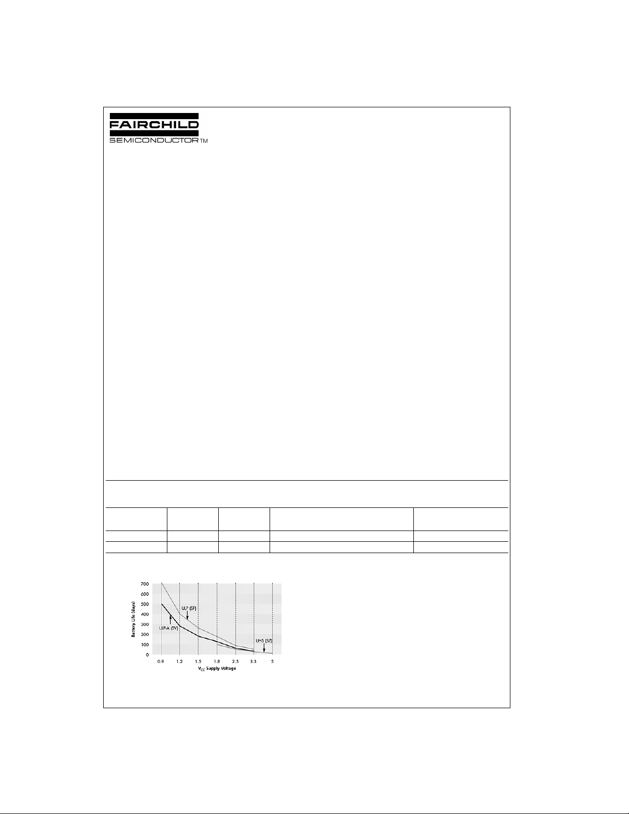
Battery Life vs. V
TinyLogic is a regist ered trademark of Fairc hild Semiconduct or Corporation.
MicroPak, and Qu iet Series are trademarks of Fairchild Semiconductor Corporation.
© 2004 Fairchild Semiconductor Corporation DS500607 www.fairchildsemi.com
Package Product Code
Number Top Mark
Supply Voltage
CC
Package Description Supplied As
TinyLogic ULP and ULP -A with up to 50% les s power consumption can
extend your battery lif e significantly.
Battery Life = (V
Where, P
device
Assumes ideal 3.6V Lithium Ion battery with current rating of 900mAH and
derated 90% and device frequency at 10MHz, wi th C
= (I
battery
*I
* VCC) + (C
CC
battery
*.9)/(P
PD
)/24hrs/day
device
+ CL) * V
CC
2
* f
= 15 pF load
L
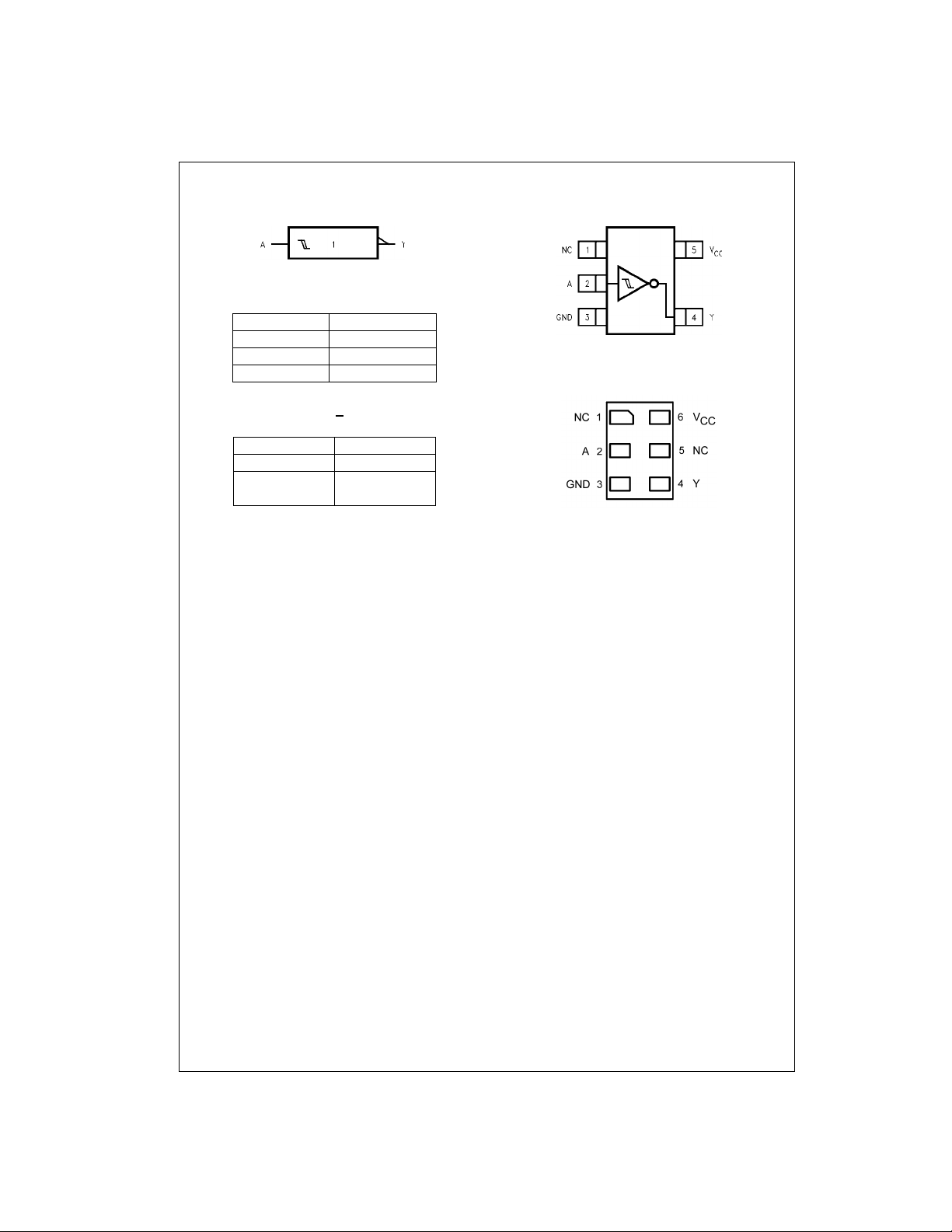
Logic Symbol
Connection Diagrams
NC7SV14
Pin Descriptions
Pin Names Description
NC No Connect
Function Table
Input Output
H = HIGH Logic Level
L = LOW Logic Level
IEEE/IEC
A Input
Y Output
Y = A
AY
LH
HL
Pin Assignments for SC70
(Top View)
Pad Assignments for MicroPak
(Top Thru View)
www.fairchildsemi.com 2
Absolute Maximum Ratings(Note 1) Recommended Operating
Supply Voltage (VCC) −0.5V to +4.6V
DC Input Voltage (V
DC Output Voltage (V
HIGH or LOW State (Note 2)
V
= 0V −0.5V to +4.6V
CC
DC Input Diode Current (I
DC Output Diode Current (I
V
< 0V −50 mA
OUT
V
> V
OUT
CC
DC Output Source/Sink Current (I
DC V
or Ground Current per
CC
Supply Pin (I
Storage Temperature Range (T
) −0.5V to +4.6V
IN
)
OUT
) VIN < 0V ±50 mA
IK
)
OK
or Ground) ± 50 mA
CC
STG
−0.5V to V
) ± 50 mA
OH/IOL
CC
) −65°C to +150°C
+0.5V
+50 mA
Conditions
Supply Voltage 0.9V to 3.6V
Input Voltage (V
Output Voltage (V
= 0.0V 0V to 3.6V
V
CC
HIGH or LOW State 0V to V
Output Current in IOH/I
VCC = 3.0V to 3.6V ±24 mA
V
= 2.3V to 2.7V ±18 mA
CC
V
= 1.65V to 1.95V ±6 mA
CC
= 1.4V to 1.6V ±4 mA
V
CC
V
= 1.1V to 1.3V ±2 mA
CC
V
= 0.9V ±0.1 mA
CC
Free Air Operating Temperature (T
Minimum Input Edge Rate (
V
= 0.8V to 2.0V, VCC = 3.0V 10 ns/V
IN
Note 1: Absolute Maximum Ratings: are those values beyond which the
safety of the device can not be gu arant eed. The de vice sh ould no t be operated at these limits. The parametric values defined in the Electrical Characteristics tables are not guaranteed at the absolute maximum ratings. The
“Recommended Operating Con ditions” table will define the conditions for
actual device opera tion.
Absolute Maximum Rating must be observed.
Note 2: I
O
Note 3: Unused inputs must be held HIGH or LOW. They may not float.
(Note 3)
) 0V to 3.6V
IN
)
OUT
OL
) −40°C to +85°C
A
∆t/∆V)
DC Electrical Characteristics
V
Symbol Parameter
V
Positive Threshold Voltage 0.90 0.3 0.7 0.3 0.7
P
V
Negative Threshold Voltage 0.90 0.10 0.6 0.10 0.6
N
V
Hysteresis Voltage 0.90 0.07 0.5 0.07 0.5
H
CC
(V) Min Max Min Max
1.10 0.4 1.0 0.4 1.0
1.40 0.5 1.4 0.5 1.4
1.65 0.7 1.5 0.7 1.5
2.30 1.0 1.8 1.0 1.8
2.70 1.3 2.2 1.3 2.2
1.10 0.15 0.7 0.15 0.7
1.40 0.20 0.8 0.20 0.8
1.65 0.25 0.9 0.25 0.9
2.30 0.4 1.15 0.4 1.15
2.70 0.6 1.5 0.6 1.5
1.10 0.08 0.6 0.08 0.6
1.40 0.10 0.8 0.10 0.8
1.65 0.15 1.0 0.15 1.0
2.30 0.25 1.1 0.25 1.1
2.70 0.40 1.2 0.40 1.2
TA = +25°CT
= −40°C to +85°C
A
Units Conditions
NC7SV14
CC
V
V
V
3 www.fairchildsemi.com

DC Electrical Characteristics (Continued)
Symbol Parameter
NC7SV14
V
HIGH Level 0.90 VCC − 0.1 VCC − 0.1
OH
Output Voltage 1.10 ≤ VCC ≤ 1.30 VCC − 0.1 VCC − 0.1
V
LOW Level 0.90 0.1 0.1
OL
Output Voltage 1.10 ≤ VCC ≤ 1.30 0.1 0.1
I
Input Leakage Current 0.90 to 3.60 ±0.1 ±0.5 µA0 ≤ VI ≤ 3.6V
IN
Power Off Leakage Current 0 0.5 0.5 µA0 ≤ (VI, VO) ≤ 3.6V
I
OFF
I
Quiescent Supply Current 0.90 to 3.60 0.9 0.9
CC
V
CC
(V) Min Max Min Max
1.40 ≤ V
≤ 1.60 VCC − 0.2 VCC − 0.2
CC
1.65 ≤ VCC ≤ 1.95 VCC − 0.2 VCC − 0.2
< 2.70 VCC − 0.2 VCC − 0.2
2.30 ≤ V
CC
2.70 ≤ V
≤ 3.60 VCC − 0.2 VCC − 0.2
CC
1.10 ≤ VCC ≤ 1.30 0.75 x V
≤ 1.60 0.75 x V
1.40 ≤ V
CC
1.65 ≤ V
≤ 1.95 1.25 1.25
CC
2.30 ≤ V
< 2.70 2.0 2.0
CC
< 2.70 1.8 1.8
2.30 ≤ V
CC
2.70 ≤ V
≤ 3.60 2.2 2.2
CC
< 2.70 1.7 1.7
2.30 ≤ V
CC
2.70 ≤ VCC ≤ 3.60 2.4 2.4
TA = +25°CT
CC
CC
= −40°C to +85°C
A
0.75 x V
CC
0.75 x V
CC
Units Conditions
= −100 µA
I
OH
IOH = −2 mA
IOH = −4 mA
V
= −6 mA
I
OH
IOH = −12 mA
IOH = −18 mA
2.70 ≤ VCC ≤ 3.60 2.2 2.2 IOH = −24 mA
1.40 ≤ VCC ≤ 1.60 0.2 0.2
1.65 ≤ VCC ≤ 1.95 0.2 0.2
IOL = 100 µA
2.30 ≤ VCC < 2.70 0.2 0.2
2.70 ≤ VCC ≤ 3.60 0.2 0.2
1.10 ≤ VCC ≤ 1.30 0.25 x V
1.40 ≤ VCC ≤ 1.60 0.25 x V
CC
CC
0.25 x V
0.25 x V
V
IOL = 2 mA
IOL = 4 mA
CC
CC
1.65 ≤ VCC ≤ 1.95 0.3 0.3 IOL = 6 mA
2.30 ≤ VCC < 2.70 0.4 0.4
≤ 3.60 0.4 0.4
2.70 ≤ V
CC
2.30 ≤ V
< 2.70 0.6 0.6
CC
2.70 ≤ VCC ≤ 3.60 0.4 0.4
I
OL
I
OL
= 12 mA
= 18 mA
2.70 ≤ VCC ≤ 3.60 0.55 0.55 IOL = 24 mA
VI = VCC or GND
0.90 to 3.60 ±0.9 V
µA
≤ VI ≤ 3.6V
CC
AC Electrical Characteristics
V
Symbol Parameter
t
Propagation Delay 0.90 12
PHL
t
PLH
CC
(V) Min Typ Max Min Max
1.10 ≤ VCC ≤ 1.30 2.0 5.9 10.0 1.0 14.9 CL = 15 pF, RL = 2 kΩ
1.40 ≤ VCC ≤ 1.60 1.0 3.2 6.1 0.9 7.0
1.65 ≤ VCC ≤ 1.95 1.0 2.0 5.2 0.7 6.2 CL = 30 pF
2.30 ≤ VCC < 2.70 0.8 1.8 3.7 0.6 4.4 RL = 500Ω
2.70 ≤ VCC ≤ 3.60 0.7 1.5 3.3 0.5 3.8
C
Input Capacitance 0 2.0 pF
IN
C
Output Capacitance 0 4.5 pF
OUT
C
Power Dissipation
PD
Capacitance f = 10 MHz
0.90 to 3.60 10 pF
www.fairchildsemi.com 4
TA = +25°CT
= −40°C to +85°C
A
Units Conditions
CL = 15 pF, RL = 1 MΩ
ns
VI = 0V or V
CC
Figure
Number
Figures
1, 2

AC Loading and Waveforms
Symbol
V
mi
V
mo
3.3V ± 0.3V 2.5V ± 0.2V 1.8V ± 0.15V 1.5V ± 0.10V 1.2V ± 0.10V 0.9V
1.5V VCC/2 VCC/2 VCC/2 VCC/2 VCC/2
1.5V VCC/2 VCC/2 VCC/2 VCC/2 VCC/2
FIGURE 1. AC Test Circuit
FIGURE 2. AC Waveforms
V
CC
NC7SV14
5 www.fairchildsemi.com

Tape and Reel Specification
TAPE FORMAT for SC70
Package Tape Number Cavity Cover Tape
Designator Section Cavities Status Status
NC7SV14
P5X Carrier 3000 Filled Sealed
TAPE DIMENSIONS inches (millimeters)
Leader (Start End) 125 (typ) Empty Seal ed
Trailer (Hub End) 75 (typ) Empty Sealed
www.fairchildsemi.com 6
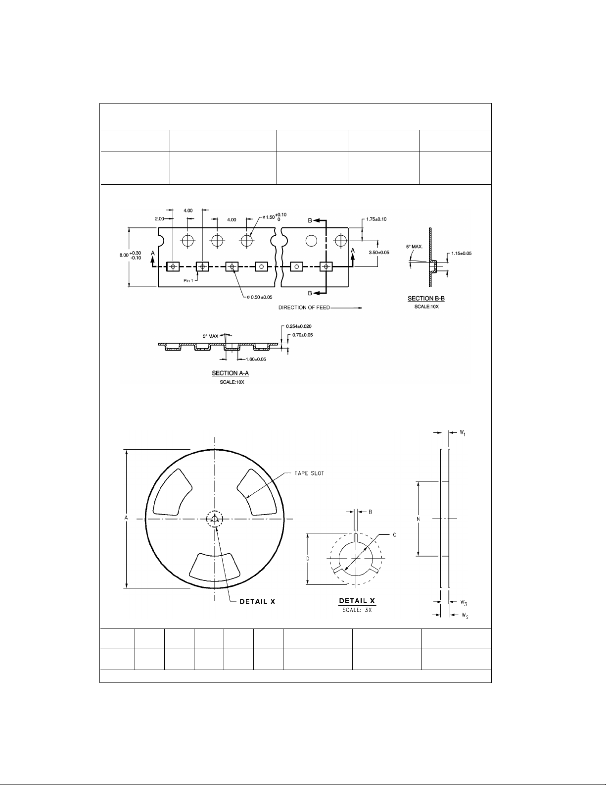
Tape and Reel Specification (Continued)
TAPE FORMAT for MicroPak
Package Tape Number Cavity Cover Tape
Designator Section Cavities Status Status
Leader (Start End) 125 (typ) Empty Sealed
L6X Carrier 5000 Filled Sealed
Trailer (Hub End) 75 (typ) Empty Sealed
TAPE DIMENSIONS inches (millimeters)
NC7SV14
REEL DIMENSIONS inches (millimeters)
Tape
Size
8 mm
ABCDN W1 W2 W3
7.0 0.059 0.512 0.795 2.165 0.331
(177.8) (1.50) (13.00) (20.20) (55.00) (8.40
+ 0.059/−0.000 0.567 W1 + 0.078/−0.039
+ 1.50/−0.00) (14.40) (W1 + 2.00/−1.00)
7 www.fairchildsemi.com

Physical Dimensions inches (millimeters) unless otherwise noted
NC7SV14
5-Lead SC70, EIAJ SC-88a, 1.25mm Wide
Package Number MAA05A
www.fairchildsemi.com 8

Physical Dimensions inches (millimeters) unless otherwise noted (Continued)
NC7SV14 TinyLogic
ULP-A Inverter with Schmitt Trigger Input
6-Lead MicroPak, 1.0mm Wide
Package Number MAC06A
Fairchild does not assume any responsibility for use of any circuitry described , no circuit patent licenses are implied and
Fairchild reserves the right at any time without notice to change said circuitry and specifications.
LIFE SUPPORT POLICY
FAIRCHILD’S PRODUCTS ARE NOT AUTHORIZED FOR USE AS CRITICAL COMPONENTS IN LIFE SUPPORT
DEVICES OR SYSTEMS WITHOUT THE EXPRESS WRITTEN APPROVAL OF THE PRESIDENT OF FAIRCHILD
SEMICONDUCTOR CORPORATION. As used herein:
1. Life support devices or systems are dev ic es or syste ms
which, (a) are intended for surgical implant into the
body, or (b) support or sustain life, and (c) whose failure
to perform when properly used in accordance with
instructions for use provide d in the l abe ling, can be reasonably expected to result in a significant injury to the
user.
2. A critical compo nent in any com ponen t of a life s upp ort
device or system whose failure to perform can be reasonably expected to cause the failure of the life support
device or system, or to affect its safety or effectiveness.
www.fairchildsemi.com
9 www.fairchildsemi.com
 Loading...