Fairchild NC7SV00 service manual

®
NC7SV00
TinyLogic
®
ULP-A 2-Input NAND Gate
NC7SV00 — TinyLogic
November 2010
ULP-A 2-Input NAND Gate
Features
0.9V to 3.6V V
Supply Operation
CC
3.6V Over-Voltage Tolerant I/Os at VCC from
0.9V to 3.6V
Extremely High Speed tPD
- 1.0ns: Typical for 2.7V to 3.6V V
- 1.2ns: Typical for 2.3V to 2.7V V
- 2.0ns: Typical for 1.65V to 1.95V VCC
- 3.2ns: Typical for 1.4V to 1.6V V
- 6.0ns: Typical for 1.1V to 1.3V V
- 13.0ns: Typical for 0.9V V
CC
CC
CC
CC
CC
Power-Off High-Impedance Inputs and Outputs
High Static Drive (I
- ±24mA at 3.00V V
- ±18mA at 2.30V V
- ±6mA at 1.65V V
- ±4mA at 1.4V V
- ±2mA at 1.1V V
- ±0.1mA at 0.9V V
OH/IOL
CC
CC
CC
CC
CC
CC
)
Uses Proprietary Quiet Series™ Noise/EMI
Reduction Circuitry
Ultra-Small MicroPak™ Packages
Ultra-Low Dynamic Power
Description
The NC7SV00 is a single two-input NAND gate from
Fairchild's Ultra-Low Power (ULP-A) Series of
TinyLogic
extreme high speed, high drive, and low power. This
product is designed for a wide low-voltage operating
range (0.9V to 3.6V V
more drive and speed than the TinyLogic
but still offer best-in-class, low-power operation.
The NC7SV00 is uniquely designed for optimized power
and speed and is fabricated with an advanced CMOS
technology to achieve high-speed operation while
maintaining low CMOS power dissipation.
®.
ULP-A is ideal for applications that require
) and applications that require
CC
®
ULP series,
Ordering Information
Part Number Top Mark Package Packing Method
NC7SV00P5X V00 5-Lead SC70, EIAJ SC-88a, 1.25mm Wide 3000 Units on Tape & Reel
NC7SV00L6X F5 6-Lead MicroPak™, 1.00mm Wide 5000 Units on Tape & Reel
NC7SV00FHX F5 6-Lead, MicroPak2™, 1x1mm Body, .35mm Pitch 5000 Units on Tape & Reel
TinyLogic® is a registered trademark of Fairchild Semiconductor Corporation.
MicroPak™ and Quiet Series™ are trademarks of Fairchild Semiconductor Corporation.
© 2002 Fairchild Semiconductor Corporation www.fairchildsemi.com
NC7SV00 • Rev. 1.0.3

®
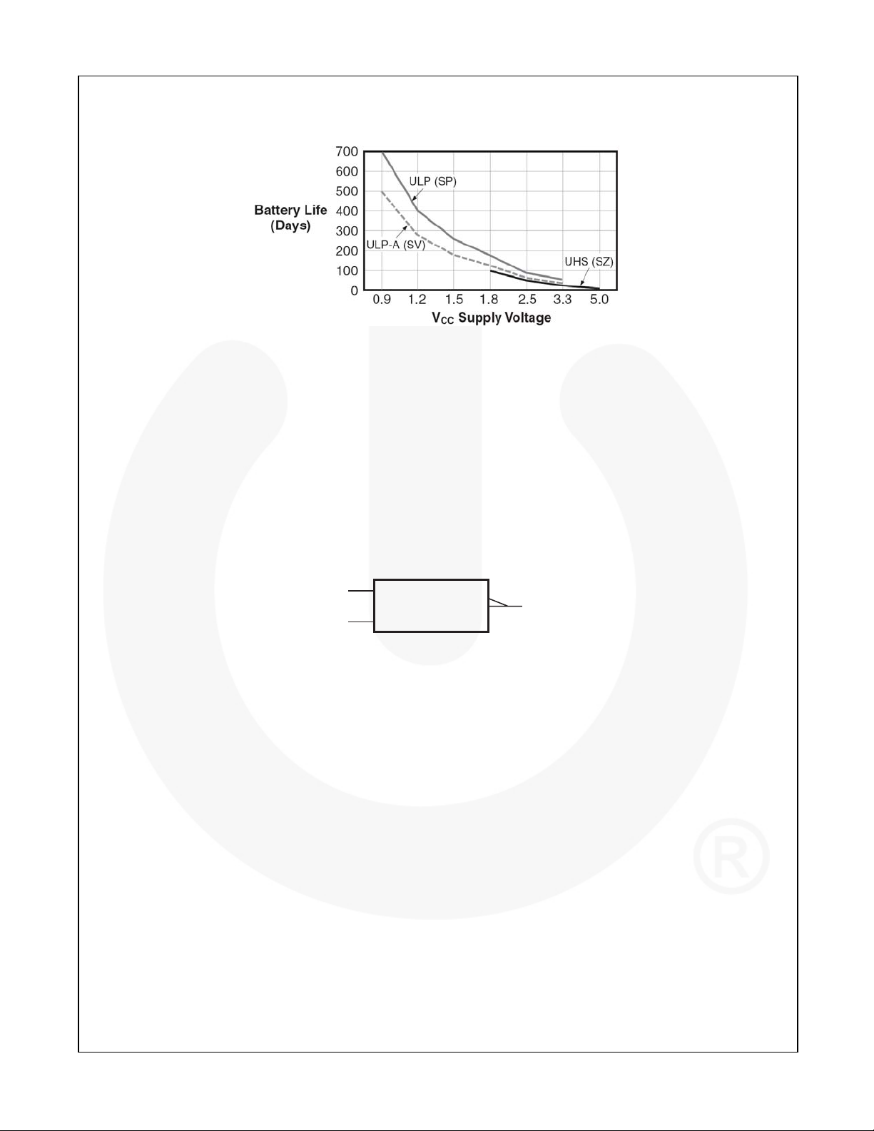
Battery Life
Figure 1. Battery Life vs. V
Supply Voltage
CC
NC7SV00 — TinyLogic
ULP-A 2-Input NAND Gate
Notes:
1. TinyLogic
Battery Life = (V
where, P
®
ULP and ULP-A with up to 50% less power consumption can extend battery life significantly.
device
battery•Ibattery
= (I
CC
• V
CC
•.9)/(P
) + (C
PD
+ C
)/24hrs/day
device
) • V
L
CC2
• f.
2. Assumes ideal 3.6V Lithium Ion battery with current rating of 900mAH and derated 90% and device frequency at
10MHz, with C
=15pF load.
L
Connection Diagram
IEEE/IEC
A
B
&
Figure 2. Logic Symbol
Y
© 2002 Fairchild Semiconductor Corporation www.fairchildsemi.com
NC7SV00 • Rev. 1.0.3 2

®
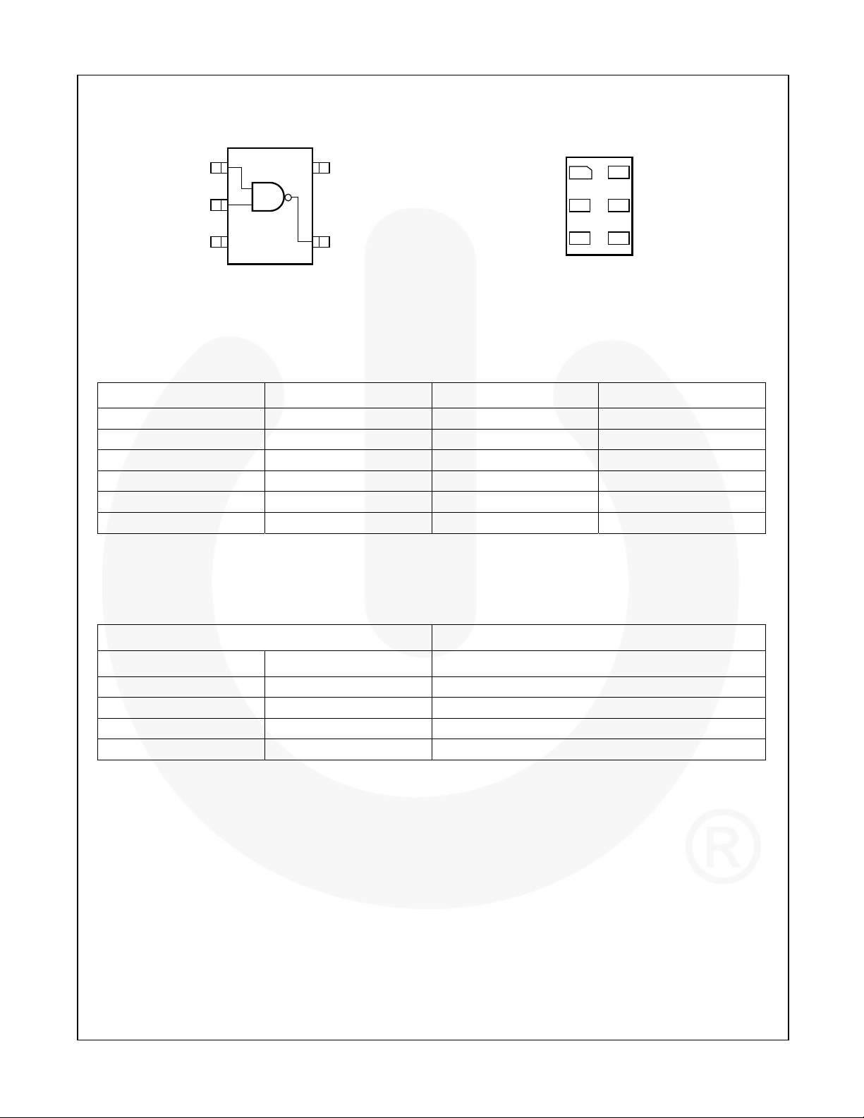
Pin Configurations
NC7SV00 — TinyLogic
A
B
GND
Figure 3. SC70 (Top View) Figure 4. MicroPak™ (Top Through View)
Pin Definitions
Pin # SC70 Pin # MicroPak™ Name Description
1 1 A Input
2 2 B Input
3 3 GND Ground
4 4 Y Output
5 NC No Connect
5 6 VCC Supply Voltage
1
2
3 4
5
V
CC
Y
GND
1
A
2
B
3
6
V
CC
5
NC
4
Y
ULP-A 2-Input NAND Gate
Function Table
A B Y
L L H
L H H
H L H
H H L
H=HIGH Logic Level
L=LOW Logic Level
Inputs Output
© 2002 Fairchild Semiconductor Corporation www.fairchildsemi.com
NC7SV00 • Rev. 1.0.3 3

®
NC7SV00 — TinyLogic
Absolute Maximum Ratings
Stresses exceeding the absolute maximum ratings may damage the device. The device may not function or be
operable above the recommended operating conditions and stressing the parts to these levels is not recommended.
In addition, extended exposure to stresses above the recommended operating conditions may affect device
reliability. The absolute maximum ratings are stress ratings only.
Symbol Parameter Min. Max. Unit
VCC Supply Voltage -0.5 4.6 V
VIN DC Input Voltage -0.5 4.6 V
(3)
V
DC Output Voltage
OUT
HIGH or LOW State
VCC=0V -0.5 4.6
IIK DC Input Diode Current VIN < 0V -50 mA
< 0V -50
V
IOK DC Output Diode Current
I
DC Output Source/Sink Current ±50 mA
OH/IOL
ICC or I
DC VCC or Ground Current per Supply Pin ±50 mA
GND
T
Storage Temperature Range -65 +150 °C
STG
OUT
V
> VCC +50
OUT
TJ Junction Temperature Under Bias +150 °C
TL Junction Lead Temperature, Soldering 10 Seconds +260 °C
SC70-5 150
PD Power Dissipation at +85°C
MicroPak2™-6 120
ESD
Human Body Model, JEDEC:JESD22-A114 4000
Charge Device Model, JEDEC:JESD22-C101 2000
Note:
3. IO absolute maximum rating must be observed.
-0.5 VCC + 0.5
V
ULP-A 2-Input NAND Gate
mA
mW MicroPak™-6 130
V
Recommended Operating Conditions
The Recommended Operating Conditions table defines the conditions for actual device operation. Recommended
operating conditions are specified to ensure optimal performance to the datasheet specifications. Fairchild does not
recommend exceeding them or designing to Absolute Maximum Ratings.
Symbol Parameter Conditions Min. Max. Unit
VCC Supply Voltage 0.9 3.6 V
VIN Input Voltage 0 3.6 V
V
Output Voltage
OUT
IOH/IOL Output Current in IOH/IOL
TA Operating Temperature, Free Air -40 +85 °C
Δt/ΔV
θ
JA
Minimum Input Edge Rate V
Thermal Resistance
Note:
4. Unused inputs must be held HIGH or LOW. They may not float.
© 2002 Fairchild Semiconductor Corporation www.fairchildsemi.com
NC7SV00 • Rev. 1.0.3 4
VCC=0V 0 3.6
HIGH or LOW State 0 VCC
V
=3.0V to 3.6V ±24.0
CC
V
VCC=2.3V to 3.6V ±18.0
VCC=1.65V to 1.95V ±6.0
VCC=1.4V to 1.6V ±4.0
mA
VCC=1.1V to 1.3V ±2.0
VCC=0.9V ±0.1
=0.8V to 2.0, VCC=3.0V 10 ns/V
IN
SC70-5 425
°C/W MicroPak™-6 500
MicroPak2™-6 560
 Loading...