

NC7SU04
NC7SU04 TinyLogic
October 1995
Revised August 2004
TinyLogic
General Description
The NC7SU04 is a singl e special pu rpose CMOS Inverter.
The inverter circuit is designed with a single unbuffered
stage to facilitate use in crystal oscillator applications. It is
not intended for use in logic inversion applications.
Advanced Silicon Gate CMOS fabrication assures high
speed and low pow er circuit operation over a broad V
range. ESD protecti on diodes inherently guard both input
and output with respect to the V
HS Unbuffered Inverter
Features
■ Space saving SOT23 or SC70 5-lead package
■ Ultra small MicroPak
■ Unbuffered for crystal oscillator applications
■ Low Quiescent Power; I
■ Balanced Output Drive; 2 mA I
CC
and GND rails.
CC
■ Broad VCC Operating Range; 2V–6V
■ Balanced Propagation Dela ys
■ Specified for 3V operation
leadless package
< 1 µA
CC
, −2 mA I
OL
OH
Ordering Code:
Order Number
NC7SU04M5X MA05B 7SU4 5-Lead SOT23, JEDEC MO-178, 1.6mm 3k Units on Tape and Reel
NC7SU04P5X MAA05A SU4 5-Lead SC70, EIAJ SC-88a, 1.25mm Wide 3k Units on Tape and Reel
NC7SU04L6X MAC06A E5 6-Lead MicroPak, 1.0mm Wide 5k Units on Tape and Reel
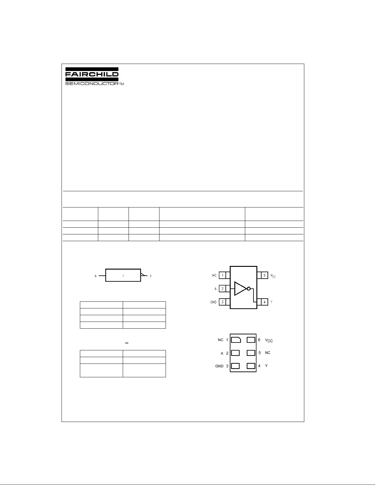
Logic Symbol
Package Product Code
Number Top Mark
IEEE/IEC
Package Description Supplied As
Connection Diagrams
Pin Assignme nts for SOT23 and SC70
HS Unbuffered Inverter
Pin Descriptions
Pin Names Description
A Input
Y Output
NC No Connect
Pad Assignments for MicroPak
(Top View)
Function Table
Y
= A
Input Output
AY
LH
HL
H = HIGH Logic Le v el
L = LOW Logic Level
TinyLogic is a registered tradema rk of F airc hild Semiconduct or Corporation.
MicroPak are trad em arks of Fairchild Sem ic onductor Corporation.
© 2004 Fairchild Semiconductor Corporation DS012142 www.fairchildsemi.com
(Top Thru View)
Absolute Maximum Ratings(Note 1) Recommended Operating
Supply Voltage (VCC) −0.5V to +7.0V
DC Input Diode Current (I
NC7SU04
@ V
≤ −0.5V −20 mA
IN
≥ VCC +0.5V +20 mA
@ V
IN
DC Input Voltage (V
DC Output Diode Current (I
< −0.5V −20 mA
@ V
OUT
@ V
> VCC +0.5V +20 mA
OUT
DC Output Voltage (V
)
IK
) −0.5V to VCC + 0.5V
IN
)
OK
) −0.5V to VCC + 0.5V
OUT
DC Output Source
or Sink Current (I
DC V
or Ground Current
CC
per Output Pin (I
Storage Temperature (T
Junction Temperature (T
Lead Temperature (T
) ±12.5 mA
OUT
or I
CC
) ±25 mA
GND
) −65°C to +150°C
STG
)150°C
J
);
L
(Soldering, 10 seconds) 260
Conditions
Supply Voltage (V
Input Voltage (V
Output Voltage (V
Operating Temperature (TA) −40°C to +85°C
Thermal Resistance (
SOT23-5 300
SC70-5 425
Note 1: Absolute maximum ratings are those values beyond which damage
to the device may occur. The databook specifications should be met, without exception, to ensure that the system design is reliable over its power
supply, temperature, and ou tput/inp ut loadi ng varia bles. Fairchild does no t
recommend operat ion of circuits outside databook specific at ions.
Note 2: Unused inputs must be held HIGH or LOW. They may not float.
°C
(Note 2)
) 2.0V to 6.0V
CC
) 0V to V
IN
) 0V to V
OUT
θ
)
JA
DC Electrical Characteristics
V
Symbol Parameter
HIGH Level Input Voltage 2.0 1.70 1.70
V
IH
V
LOW Level Input Voltage 2.0 0.30 0.30
IL
V
HIGH Level Output Voltage 2.0 1.80 2.0 1.80
OH
V
LOW Level Output Voltage 2.0 0.00 0.20 0.20
OL
I
Input Leakage Current 6.0 ±0.1 ±1.0 µAVIN = VCC, GND
IN
I
Quiescent Supply Current 6.0 1.0 10.0 µAVIN = VCC, GND
CC
CC
(V) Min Typ Max Min Max
3.0 2.45 2.45
4.5 3.60 3.60
6.0 4.80 4.80
3.0 0.50 0.50
4.5 0.90 0.90
6.0 1.20 1.20
3.0 2.5 3.0 2.50 I
4.5 4.00 4.5 4.00 VIN = V
6.0 5.50 5.9 5.50
3.0 2.68 2.82 2.63 IOH = −1.3 mA
4.5 4.18 4.33 4.13 IOH = −2 mA
6.0 5.68 5.76 5.63 IOH = −2.6 mA
3.0 0.00 0.50 0.50 IOL = 20 µA
4.5 0.01 0.50 0.50 VIN = V
6.0 0.04 0.50 0.50
3.0 0.11 0.26 0.33 IOL = 1.3 mA
4.5 0.12 0.26 0.33 IOL = 2 mA
6.0 0.15 0.26 0.33 IOL = 2.6 mA
TA = +25°CT
= −40°C to +85°C
A
Units Conditions
V
V
= −20 µA
OH
V
V
V
V
= GND
V
IN
VIN = V
IL
IH
CC
CC
CC
°C/W
°C/W
www.fairchildsemi.com 2
AC Electrical Characteristics
V
Symbol Parameter
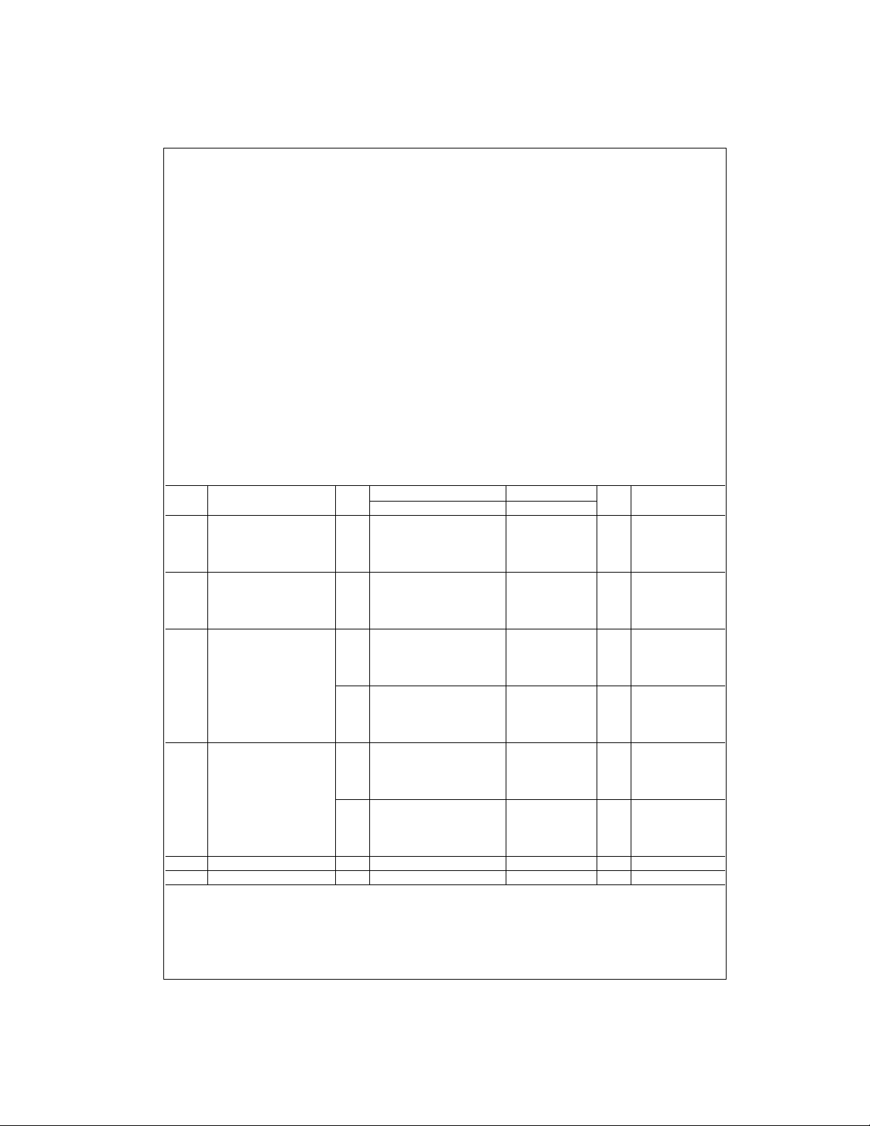
t
, Propagation Delay 5.0 3 15 ns CL = 15 pF
PLH
t
PHL
CC
(V) Min Typ Max Min Max Number
2.0 17 100 125
3.0 9 27 35
4.5 7 20 25
6.0 6.5 17 21
t
, Output Transition Time 5.0 4 10 ns CL = 15 pF
TLH
t
THL
2.0 25 125 155
3.0 16 35 45
4.5 12 25 31
6.0 10 21 26
CIN Input Capacitance Open 2 10 10 pF
C
Power Dissipation Capacitance 5.0 4 pF (Note 3) Figure 2
PD
Note 3: CPD is defined as the value of the internal equivalent capacitance which is derived from dynamic operating current consumption (I
loading and operating at 50% duty cycle. (See Figure 2.) C
= (CPD)(VCC)(fIN) + (ICCstatic).
I
CCD
TA = +25°CT
is related to I
PD
dynamic operating current by the express ion:
CCD
= −40°C to +85°C
A
Units Conditions
CL = 50 pF
ns
CL = 50 pF
ns
AC Loading and Waveforms
) at no output
CCD
Figure
Figures
1, 3
Figures
1, 3
NC7SU04
CL includes load and s tr ay c apacitance
Input PR R = 1.0 MHz; t
= 500 ns
W
FIGURE 1. AC Test Circuit
Input = AC Wavefor m;
PRR = variable; Duty Cycle = 50%
FIGURE 2. I
CCD
FIGURE 3. AC Waveforms
Test Circuit
3 www.fairchildsemi.com
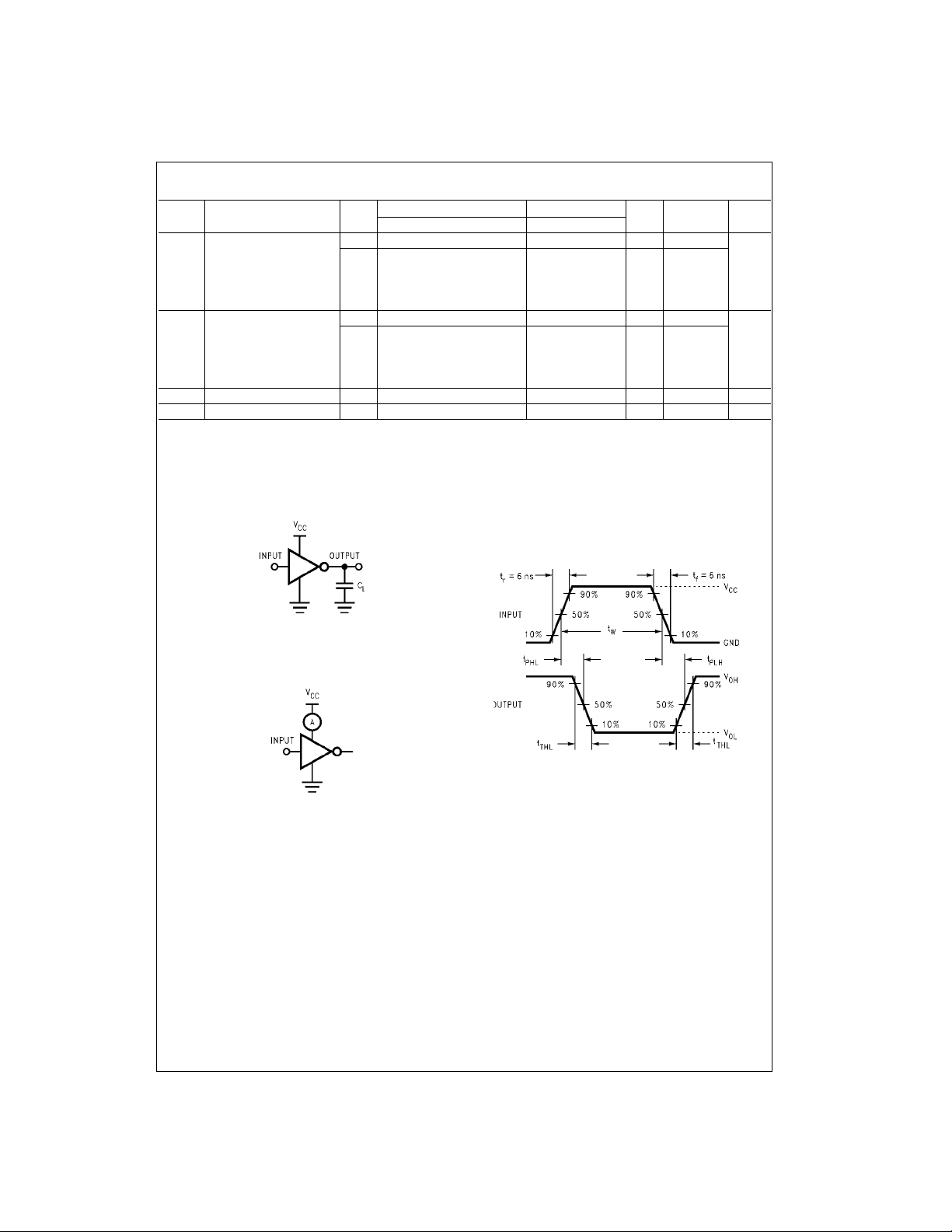
Tape and Reel Specification
TAPE FORMAT for SOT23 and SC70
Package Tape Number Cavity Cover Tape
Designator Section Cavities Status Status
NC7SU04
M5X, P5X Carrier 3000 Filled Sealed
TAPE DIMENSIONS inches (millimeters)
Leader (Start End) 125 (typ) Empty Sealed
Trailer (Hub End) 75 (typ) Empty Sealed
Package
SC70-5 8 mm
SOT23-5 8 mm
www.fairchildsemi.com 4
Tape Size DIM A DIM B DIM F DIM K
0.093 0.096 0.138
(2.35) (2.45) (3.5
0.130 0.130 0.138
(3.3) (3.3) (3.5
DIM P1 DIM W
o
± 0.004 0.053 ± 0.004 0.157 0.315 ± 0.004
± 0.10) (1.35 ± 0.10) (4) (8 ± 0.1)
± 0.002 0.055 ± 0.004 0.157 0.315 ± 0.012
± 0.05) (1.4 ± 0.11) (4) (8 ± 0.3)
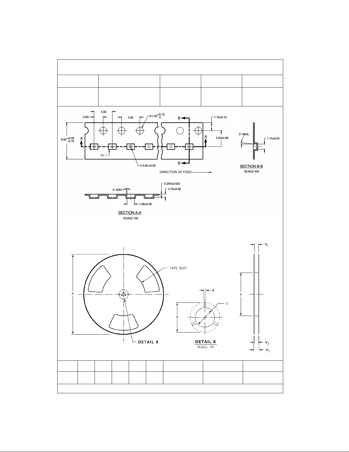
Tape and Reel Specification (Continued)
TAPE FORMAT for MicroPak
Package Tape Number C a vit y Cover Tape
Designator Section Cavities Status Status
Leader (Start End) 125 (typ) Empty Sealed
L6X Carrier 5000 Filled Sealed
Trailer (Hub End) 75 (typ) Empty Sealed
NC7SU04
REEL DIMENSIONS inches (millimeters)
Tape
Size
8 mm
ABCDN W1 W2 W3
7.0 0.059 0.512 0.795 2.165 0.331
(177.8) (1.50) (13.00) (20.20) (55.00) (8.40
+ 0.059/−0.000 0.567 W1 + 0.078/−0.039
+ 1.50/−0.00) (14.40) (W1 + 2.00/−1.00)
5 www.fairchildsemi.com

Physical Dimensions inches (millimeters) unless otherwise noted
NC7SU04
5-Lead SOT23, JEDEC MO-178, 1.6mm
Package Number MA05B
www.fairchildsemi.com 6
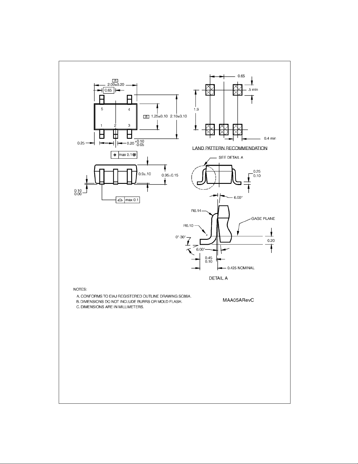
Physical Dimensions inches (millimeters) unless otherwise noted (Continued)
NC7SU04
5-Lead SC70, EIAJ SC-88a, 1.25mm Wide
Package Number MAA05A
7 www.fairchildsemi.com

Physical Dimensions inches (millimeters) unless otherwise noted (Continued)
HS Unbuffered Inverter
NC7SU04 TinyLogic
6-Lead MicroPak, 1.0mm Wide
Package Number MAC06A
Fairchild does not assume any responsibility for use of any circuitr y described, no circuit patent licenses are implied a nd
Fairchild reserves the right at any time without notice to change said circuitry and specifications.
LIFE SUPPORT POLICY
FAIRCHILD’S PRODUCTS ARE NOT AUTHORIZED FOR USE AS CRITICAL COMPONENTS IN LIFE SUPPORT
DEVICES OR SYSTEMS WITHOUT THE EXPRESS WRITTEN APPROVAL OF THE PRESIDENT OF FAIRCHILD
SEMICONDUCTOR CORPORATION. As used herein:
1. Life support devices or systems are device s or syste ms
which, (a) are intended for surgical implant into the
body, or (b) support or sustain life, and (c) whose failure
to perform when properly used in accordance with
instructions for use provided in the labeling, can be reasonably expected to result in a significant inju ry to the
user.
www.fairchildsemi.com 8
2. A critical component in any compon ent of a l ife supp ort
device or system whose failu re to perform can be reasonably expected to cause the failure of the li fe su pp ort
device or system, or to affect its safety or effectiveness.
www.fairchildsemi.com
 Loading...