Fairchild NC7SBU3157, FSAU3157 service manual

查询FSAU3157P6X供应商
NC7SBU3157 • FSAU3157
NC7SBU3157 • FSAU3157 TinyLogic
April 2002
Revised January 2003
TinyLogic
with
General Description
The NC7SBU3157 or FS AU3157 is a high performance,
single-pole/double-throw (SPDT) Analog Switch or 2:1 Multiplexer/Demultiplexer Bus Switch from Fairchild’s Ultra
High Speed Series of TinyLogic
with advanced sub-micron CMOS technology to achieve
high speed enable and d isable times and low On Resistance. The break before make sele ct circu i try prev ent s di sruption of signals on the B Port due to both switches
temporarily being enabl ed during se lect pin switchi ng. The
device is specified to op erate over the 1.65 to 5.5V V
operating range. T he control input to lerates volt ages up to
5.5V independent of the V
Fairchild’s integrated Undershoot Hardened Circuit
(UHC
preventing voltage differentials from developing and turning the switch on.
−2V Undershoot Protection
) senses undershoot at the I/Os, and re sponds by
Low Voltage UHS SPDT Analog Switch
Features
■ Useful in both analog and digital applications
■ Space saving SC70 6-lead surface mount package
. The device is fab ricat ed
operating range.
CC
■ Low On Resistance:
■ Broad VCC operating range: 1.65V to 5.5V
■ Rail-to-Rail signal handling
■ Power down high impedance cont rol input
■ Overvoltage tolerance of control input to 7.0V
■ Break before make enable circuitry
CC
■ 250 MHz - 3dB bandwidth
< 10Ω on typ @ 3.3V V
CC
Ordering Code:
Order
Number
NC7SBU3157P6X MAA06A U7A 6-Lead SC70, EIAJ SC88, 1.25mm Wide 3k Units on Tape and Reel
FSAU3157P6X MAA06A U7A 6-Lead SC70, EIAJ SC88, 1.25mm Wide 3k Units on Tape and Reel
Package
Number
Product Code
Top Mark
Package Descript ion Supplied As
Low Voltage UHS SPDT Analog Switch with
TinyLogic is a registered tradema rk and UHC is a trademark of Fairchild Semic onductor Corporat ion.
© 2003 Fairchild Semiconductor Corporation DS500618 www.fairchildsemi.com
−
2V Undershoot Protection

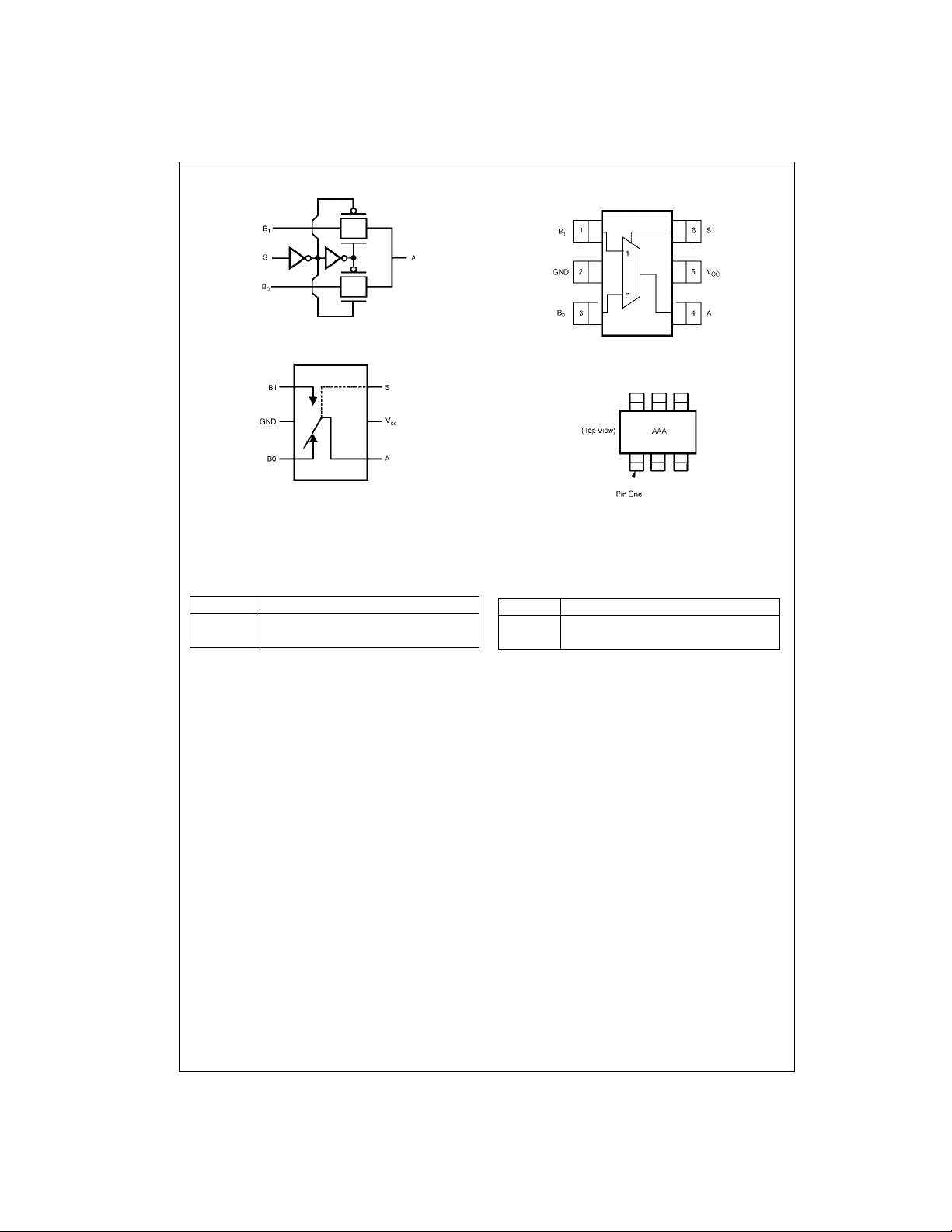
Logic Symbol
Connection Diagrams
Analog Symbol
NC7SBU3157 • FSAU3157
Function Table
Input (S) Function
LB
HB
H = HIGH Logic Level L = LOW Logic Level
Connected to A
0
Connected to A
1
(Top View)
Pin One Orientation Diagram
AAA = Product Code Top Mark - see ordering code.
Note: Orientation of Top Mark determines Pin One location. Read the top
product code mark lef t to right, Pin One is the lo w er left pin (see diagram ).
Pin Descriptions
Pin Names Description
, B
A, B
0
1
S Control Input
Data Ports
www.fairchildsemi.com 2

Absolute Maximum Ratings(Note 1) Recommended Operating
Supply Voltage (VCC) −0.5V to +7.0V
DC Switch Voltage (V
DC Input Voltage (V
DC Input Diode Current (I
@ (I
) VIN < 0V −50 mA
IK
DC Output Current (I
or Ground Current (ICC/I
DC V
CC
Storage Temperature Range (T
Junction Temperature under Bias (T
Junction Lead Temperature (T
) (Note 2) −0.5V to VCC +0.5V
S
) (Note 2) −0.5V to +7.0V
IN
)
IK
) 128 mA
OUT
) ±100 mA
GND
) −65°C to +150°C
STG
) 150°C
J
)
L
(Soldering, 10 seconds) 260
Power Dissipation (P
) @ +85°C 180 mW
D
Conditions
Supply Voltage Operating (V
Control Input Voltage (V
Switch Input Voltage (VIN)0V to V
Output Voltage (V
Operating Temperature (TA) −40°C to +85°C
Input Rise and Fall Time (t
Control Input V
Control Input V
Thermal Resistance (
Note 1: Absolute maximum ratings are DC values beyond which t he devi ce
°C
may be damag ed or hav e it s usefu l li fe i mpa ired. Th e da tas heet sp ecific ations should be met, without exception, to ensure that the system design is
reliable over its power supply, temperature, and output/input loading variables. Fairchild does not recommend operation outside datasheet specifications.
Note 2: The input and output negative voltage ratings may be exceeded if
the input and ou t put diode current ratings ar e observed.
Note 3: Control input mu s t be held HIGH or LOW, it must not float .
(Note 3)
) 1.65V to 5.5V
CC
)0V to V
IN
)0V to V
OUT
, tf)
r
= 2.3V - 3.6V 0 ns/V to 10 ns/V
CC
= 4.5V - 5.5V 0 ns/V to 5 ns/V
CC
θ
)350°C/W
JA
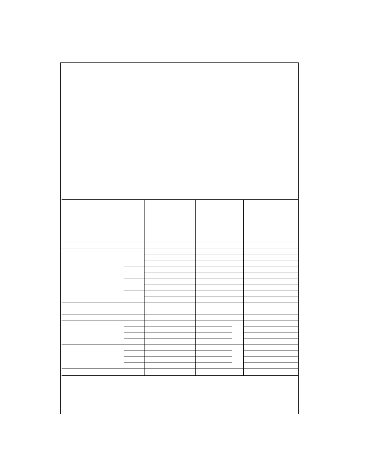
DC Electrical Characteristics
V
Symbol Parameter
V
HIGH Level 1.65 − 1.95 0.75 V
IH
Input Voltage 2.3 − 5.5 0.7 V
V
LOW Level 1.65 − 1.95 0.25 V
IL
Input Voltage 2.3 − 5.5 0.3 V
I
Input Leakage Current 0 − 5.5 ±0.05 ±0.1 ±1 µA0 ≤ VIN ≤ 5.5V
IN
OFF State Leakage Current 1.65 − 5.5 ±0.05 ±0.1 ±1 µA0 ≤ A, B ≤ V
I
OZ
R
Switch On Resistance
ON
(Note 4) 5 15 15 Ω V
I
Quiescent Supply Current
CC
All Channels ON or OFF I
Analog Signal Range V
R
On Resistance 4.5 25
RANGE
Over Signal Range 3.0 50 IA = −24 mA, 0 ≤ VBn ≤ V
(Note 4)(Note 8) 2.3 100 IA = −8 mA, 0 ≤ VBn ≤ V
∆RONOn Resistance Match 4.5 0.15
Between Channels 3.0 0.2 IA = −24 mA, VBn 2.1
(Note 4)(Note 5)(Note 6) 2.3 0.5 IA = −8 mA, VBn = 1.6
V
Voltage Undershoot 5.5 −2.0 V 0.0 mA ≥ IIN ≥ −50 mA, OE 5.5V
IKU
CC
(V) Min Typ Max Min Max
4.5
3.0
2.3
1.65
5.5 1 10 µA
CC
1.65 300 IA = −4 mA, 0 ≤ VBn ≤ V
1.65 0.5 IA = −4 mA, VBn = 1.15
TA = +25°CT
CC
CC
315 15Ω VIN = 0V, IO = 30 mA
715 15Ω V
420 20Ω VIN = 0V, IO = 24 mA
10 20 20 Ω V
530 30Ω V
13 30 30 Ω VIN = 2.3V, IO = −8 mA
6.5 50 50 Ω V
17 50 50 Ω V
0VCC0VCCV
A
0.75 V
0.7 V
CC
CC
= −40°C to +85°C
CC
CC
0.25 V
0.3 V
CC
Units Conditions
V
CC
V
= 2.4V, IO = −30 mA
IN
= 4.5V, IO = −30 mA
IN
= 3V, IO = −24 mA
IN
= 0V, IO = 8 mA
IN
= 0V, IO = 4 mA
IN
= 1.65V, IO = −4 mA
IN
VIN = VCC or GND
= 0
OUT
IA = −30 mA, 0 ≤ VBn ≤ V
Ω
IA = −30 mA, VBn = 3.15
Ω
NC7SBU3157 • FSAU3157
CC
CC
CC
CC
CC
CC
CC
CC
3 www.fairchildsemi.com
 Loading...