Fairchild NC7SB3157 service manual

查询NC7SB3157供应商
NC7SB3157
NC7SB3157 TinyLogic
January 2000
Revised June 2000
TinyLogic
Low Voltage UHS Analog Switch 2-Channel
Multiplexer/Demultiplexer
General Description
The NC7SB3157 is a high perfor mance, Anal og Switch 2channel CMOS multiplexer/demultiplexer from Fairchild’s
Ultra High Speed Series of TinyLogic
cated with advanced sub-micron CMOS technology to
achieve high spee d enable and disab le times and l ow on
resistance. The break before make select circuitry prevents
disruption of signals on the B Port due to both switches
temporarily being enabl ed during se lect pin switchi ng. The
device is specified to op erate over the 1.65 to 5.5V V
operating range. T he control input to lerates volt ages up to
5.5V independent of the V
CC
. The device is fabr i -
operating range.
Ordering Code:
Order
Number
NC7SB3157P6X MAA06A B7A 6-Lead SC70, EIAJ SC88, 1.25mm Wide 3k Units on Tape and Reel
Package
Number
Product Code
Top Mark
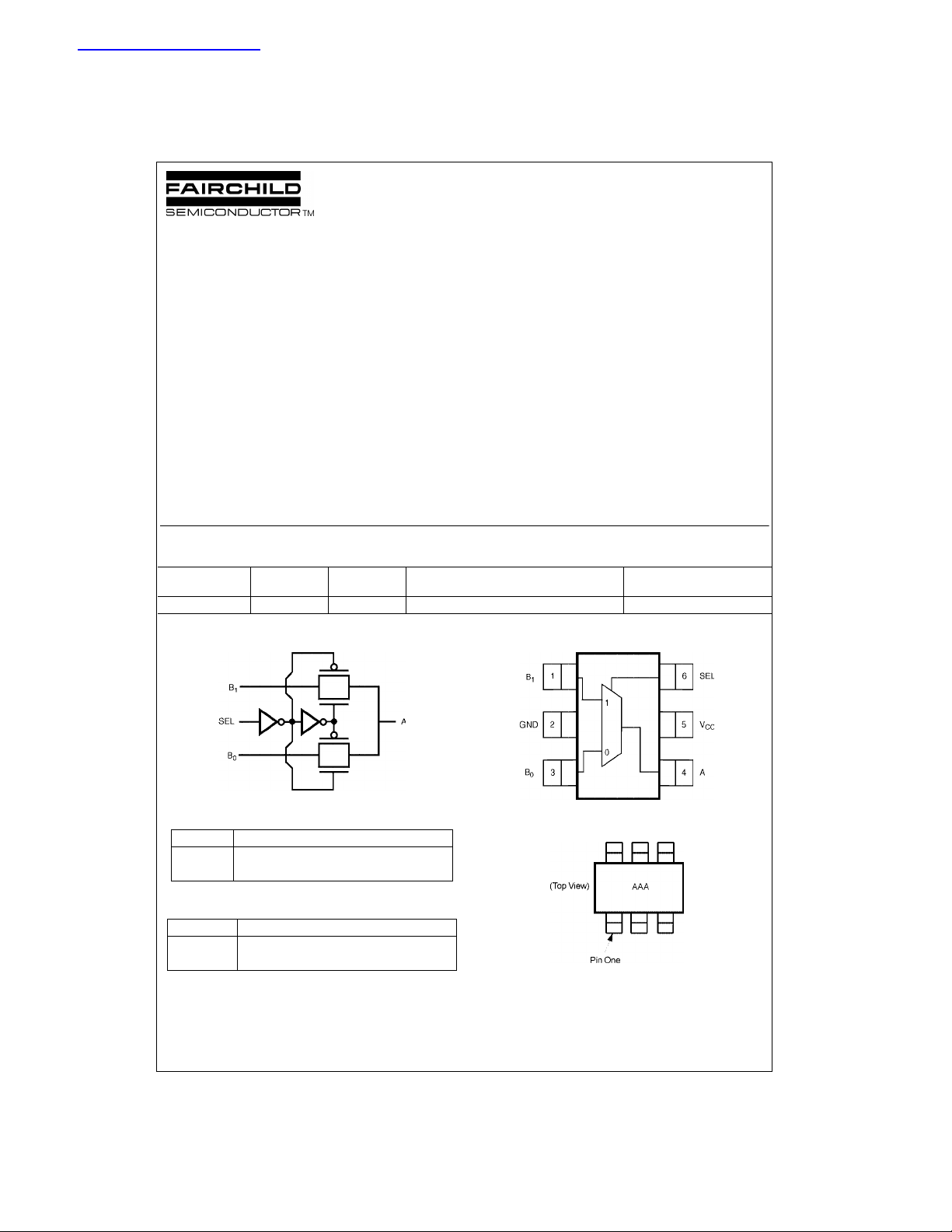
Logic Symbol
Features
■ Useful in both analog and digital applications
■ Space saving SC70 6-lead surface mount package
■ Low on resistance;
■ Broad VCC operating range; 1.65V to 5.5V
■ Power down high impedance cont rol input
■ Overvoltage tolerance of control input to 7.0V
■ Break before make enable circuitry
CC
Package Descript ion Supplied As
< 10Ω on typ @ 3.3V V
Connection Diagrams
CC
Low Voltage UHS Analog Switch 2-Channel Multiplexer/Demultiplexer
Pin Descriptions
Pin Names Description
, B
A, B
0
1
SEL Control Input
Data Ports
Pin One Orientation Diagram
(Top View)
Function Table
Input (SEL) Function
LB
HB
H = HIGH Logic Le v el
L = LOW Logic Level
TinyLogic is a trademark of Fairchild Semiconductor Co rporation.
© 2000 Fairchild Semiconductor Corporation DS500326 www.fairchildsemi.com
Connected to A
0
Connected to A
1
AAA = Product Code Top Mark - see ordering code.
Note: Orientation of Top Mark determines Pin One location. Read the top
product code mark lef t to right, Pin One is the lower left pin (see diagram ).

Absolute Maximum Ratings(Note 1) Recommended Operating
Supply Voltage (VCC) −0.5V to +7.0V
DC Switch Voltage (V
DC Input Voltage (V
NC7SB3157
DC Input Diode Current (I
@ (I
) VIN < 0V −50 mA
IK
DC Output Current (I
or Ground Current (ICC/I
DC V
CC
Storage Temperature Range (T
Junction Temperature under Bias (T
Junction Lead Temperature (T
) (Note 2) −0.5V to VCC +0.5V
S
) (Note 2) −0.5V to +7.0V
IN
)
IK
) 128 mA
OUT
) ±100 mA
GND
) −65°C to +150°C
STG
)150°C
J
)
L
(Soldering, 10 seconds) 260
Power Dissipation (P
) @ +85°C180 mW
D
Conditions
Supply Voltage Operating (V
Control Input Voltage (V
Switch Input Voltage (VIN) 0V to V
Output Voltage (V
Operating Temperature (TA) −40°C to +85°C
Input Rise and Fall Time (t
Control Input V
Control Input V
Thermal Resistance (
Note 1: Absolute maximum ratings are DC values beyond which the devi ce
°C
may be damage d or h ave its us eful life im pai red. Th e dat as heet sp ecific ations should be met, without exception, to ensure that the system design is
reliable over its power supply, temperature, and output/input loading variables. Fairchild does no t recommend operation outsid e datasheet spec ifications.
Note 2: The input and output ne gative vo ltage ra tings may be excee ded if
the input and output diode current ratings are observed.
Note 3: Control input must be held HIGH or LOW, it must not float.
(Note 3)
) 1.65V to 5.5V
CC
) 0V to V
IN
) 0V to V
OUT
, tf)
r
= 2.3V - 3.6V 0 ns/V to 10 ns/V
CC
= 4.5V - 5.5V 0 ns/V to 5 ns/V
CC
θ
)350°C/W
JA
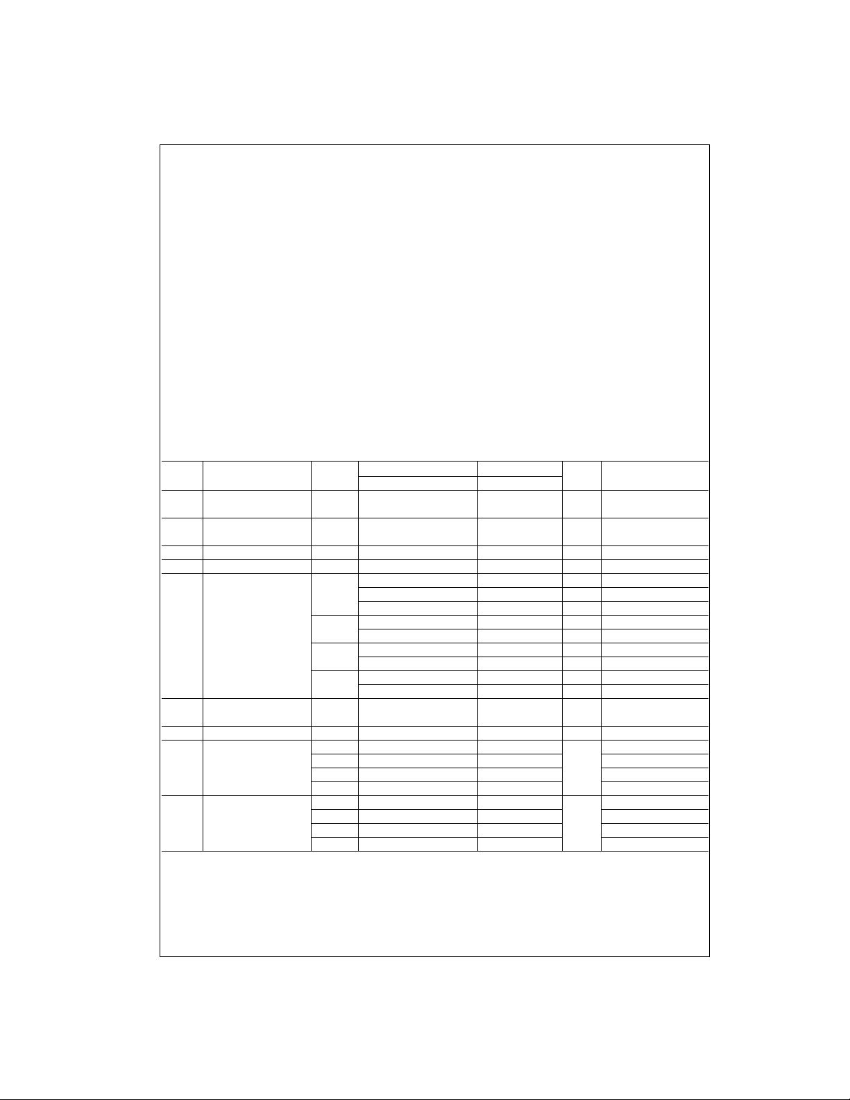
DC Electrical Characteristics
V
Symbol Parameter
V
HIGH Level 1.65 − 1.95 0.75 V
IH
Input Voltage 2.3 − 5.5 0.7 V
V
LOW Level 1.65 − 1.95 0.25 V
IL
Input Voltage 2.3 − 5.5 0.3 V
I
Input Leakage Current 0 − 5.5 ±0.1 ±1 µA0 ≤ VIN ≤ 5.5V
IN
OFF State Leakage Current 1.65 − 5.5 ±0.1 ±1 µA0 ≤ A, B ≤ V
I
OFF
R
Switch ON Resistance 4.5 3 7 7 Ω VIN = 0V, IO = 30 mA
ON
(Note 4) 5 12 12 Ω V
I
Quiescent Supply Current
CC
All Channels ON or OFF I
Analog Signal Range V
R
ON Resistance 4.5 25
RANGE
Over Signal Range 3.0 50 IA = −24 mA, 0 ≤ VBn ≤ V
(Note 4)(Note 8) 2.3 100 IA = −8 mA, 0 ≤ VBn ≤ V
∆R
ON Resistance Match 4.5 0.15
ON
Between Channels 3.0 0.2 IA = −24 mA, VBn 2.1
(Note 4)(Note 5)(Note 6) 2.3 0.5 IA = −8 mA, VBn = 1.6
CC
(V) Min Typ Max Min Max
3.0 4 9 9 Ω VIN = 0V, IO = 24 mA
2.3 5 12 12 Ω V
1.65 6.5 20 20 Ω V
5.5 1 10 µA
CC
1.65 300 IA = −4 mA, 0 ≤ VBn ≤ V
1.65 0.5 IA = −4 mA, VBn = 1.15
TA = +25°CT
CC
CC
715 15Ω V
10 20 20 Ω V
13 30 30 Ω VIN = 2.3V, IO = −8 mA
17 50 50 Ω V
0V
CC
CC
CC
= −40°C to +85°C
A
0.75 V
CC
0.7 V
CC
0.25 V
0.3 V
0VCCV
Units Conditions
V
CC
V
CC
Ω
Ω
CC
= 2.4V, IO = −30 mA
IN
= 4.5V, IO = −30 mA
IN
= 3V, IO = −24 mA
IN
= 0V, IO = 8 mA
IN
= 0V, IO = 4 mA
IN
= 1.65V, IO = −4 mA
IN
VIN = VCC or GND
= 0
OUT
IA = −30 mA, 0 ≤ VBn ≤ V
IA = −30 mA, VBn = 3.15
CC
CC
CC
CC
CC
CC
CC
www.fairchildsemi.com 2

DC Electrical Characteristics (Continued)
NC7SB3157
V
Symbol Parameter
R
On Resistance Flatness 5.0 6
flat
CC
(V) Min Typ Max Min Max
(Note 4)(Note 5)(Note 7) 3.3 12 IA = −24 mA, 0 ≤ V
2.5 28 IA = −8 mA, 0 ≤ V
1.8 125 IA = −4 mA, 0 ≤ V
Note 4: Measured by the voltage drop between A and B pins at the indicated current through the switch. On resistance is determined by the lower of the voltages on the two (A or B Po rt s ) .
Note 5: Parameter is characteri z ed but not tested in production.
Note 6: ∆R
Note 7: Flatness is defined as the difference between the maximum and minimum value of on resis t ance over the specif ied range of conditions.
Note 8: Guaranteed by Design.
= RON max − RON min measured at identical VCC, temperature and voltage levels.
ON
TA = +25°CT
= −40°C to +85°C
A
Units Conditions
IA = −30 mA, 0 ≤ V
Ω
≤ V
Bn
≤ V
Bn
≤ V
Bn
CC
≤ V
Bn
CC
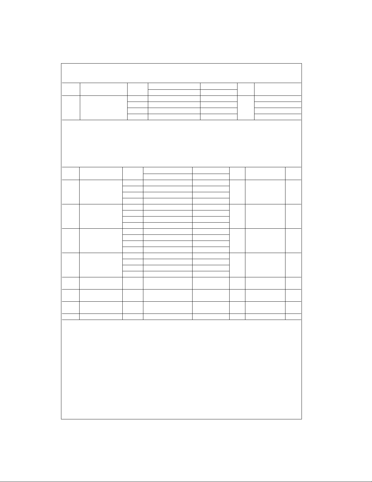
AC Electrical Characteristics
V
Symbol Parameter
t
Propagation Delay 1.65 − 1.95
PHL
Bus to Bus 2.3 − 2.7 1.2 1.2
t
PLH
CC
(V) Min Typ Max Min Max
(Note 10) 3.0 − 3.6 0.8 0.8
4.5 − 5.5 0.3 0.3
t
Output Enable Time 1.65 − 1.95 7 23 7 24
PZL
t
Turn on Time 2.3 − 2.7 3.5 13 3.5 14 VI = 2 x VCC for t
PZH
(A to Bn)3.0 − 3.6 2.5 6.9 2.5 7.6 VI = 0V for t
4.5 − 5.5 1.7 5.2 1.7 5.7
t
Output Disable Time 1.65 − 1.95 3 12.5 3 13
PLZ
t
Turn Off Time 2.3 − 2.7 2 7 2 7.5 VI = 2 x V
PHZ
(A Port to B Port) 3.0 − 3.6 1.5 5 1.5 5.3 VI = 0V for t
4.5 − 5.5 0.8 3.5 0.8 3.8
t
Break Before Make Time 1.65 − 1.95 0.5 0.5
B-M
(Note 9) 2.3 − 2.7 0.5 0.5
3.0 − 3.6 0.5 0.5
4.5 − 5.5 0.5 0.5
Q Charge Injection (Note 9) 5.0 7
3.3 3 R
OIRR Off Isolation (Note 11) 1.65 − 5.5 −57
Xtalk Crosstalk 1.65 − 5.5 −54
BW −3dB Bandwidth 1.65 − 5.5 250 MHz RL = 50Ω Figure 9
Note 9: Guaranteed by Design.
Note 10: This param eter is g uaran teed by de sign but not teste d. Th e bus switch con tribu tes no p ro pagat ion del ay o ther than the RC del ay o f the on resis-
tance of the switch and the 50 pF load capacitance, when driven b y an ideal voltage sourc e (z ero output impedanc e).
Note 11: Off Isolati o n = 20 log
[VA / VBn]
10
TA = +25°CT
= −40°C to +85°C
A
Units Conditions Fig. No.
PZL
PLZ
Figures
1, 2
Figures
1, 2
Figures
1, 2
ns VI = OPEN
ns
ns
CC
PZH
for t
PHZ
ns Figure 3
pC
dB
dB
= 0.1 nF, V
C
L
= 0Ω
GEN
R
= 50Ω
L
f = 10MHz
= 50Ω
R
L
f = 10MHz
GEN
= 0V
Figure 4
Figure 5
Figure 6
CC
CC
3 www.fairchildsemi.com
 Loading...