Fairchild NC7SB121 service manual

查询NC7SB121.pdf供应商
NC7SB121
NC7SB121 TinyLogic
October 2001
Revised October 2001
TinyLogic
Low Voltage UHS Single SPST
Wide Bandwidth Normally Open Analog Switch
General Description
The NC7SB121 is a ul tra high-speed (UHS) CM OS compatible single-pole/single-throw (SPST) analog switch or
1-bit bus switch. The LOW on resistance of the switch
allows inputs to be connected to outputs with minimal propagation delay and without generating additional ground
bounce noise. The dev ice is organized as a 1-bit switch
with a switch enable (O E) signal. When OE is HI GH, the
switch is on and Port A is connected to Port B. When OE is
LOW, the switch is open and a high-impedance state exists
between the two ports.
Ordering Code:
Order Package Product Code
Number Number Top Mark
NC7SB121M5X MA05B 7B21 5-Lead SOT23, JEDEC MO-178, 1.6mm 3k Units on Tape and Reel
NC7SB121P5X MAA05A B21 5-Lead SC70, EIAJ SC-88a, 1.25mm Wide 3k Units on Tape and Reel
NC7SB121L6X MAC06
(Preliminary)
21 6-Lead MicroPak, 1.0mm Wide 5k Units on Tape and Reel
Features
■ Space saving SOT23 or SC70 5-lead package
■ Ultra small MicroPak
■ Broad V
■ Rail-to-rail signal handling
■ 7.2
■ Minimal propagation delay through the switch
■ Low I
■ Zero bounce in flow-through mode
■ Control input compatible with CMOS input levels
■
>326 MHz −3dB bandwid th
■ Improved package replacement for the P15A121
Package Descript ion Supplied As
Operating Range 2V–5.5V
CC
Ω switch connection between two ports
CC
leadless package
Low Voltage UHS Single SPST Wide Bandwidth Normally Open Analog Switch
TinyLogic and MicroPak are trademarks of Fairchild Semico nductor Corporatio n.
© 2001 Fairchild Semiconductor Corporation DS500662 www.fairchildsemi.com

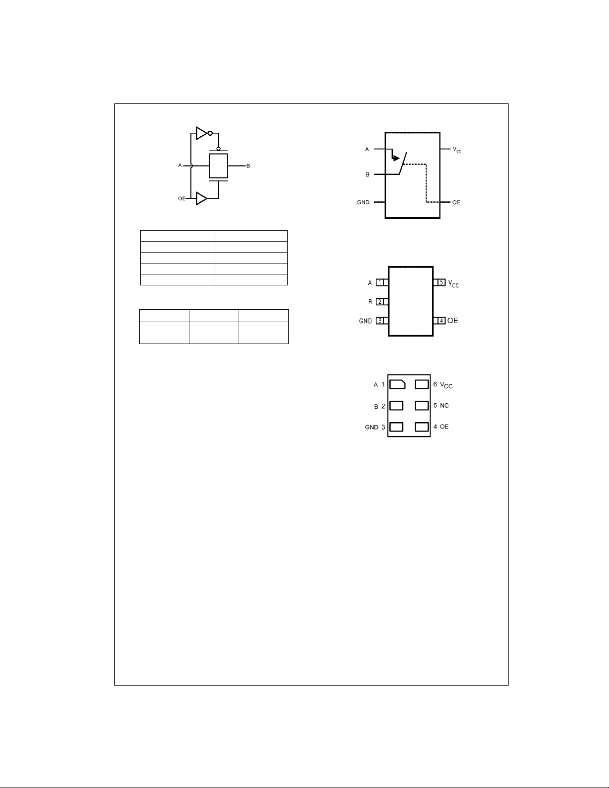
Logic Symbol
NC7SB121
Pin Descriptions
Pin Names Description
OE Switch Enable Input
NC No Connect
Function Table
OE B
L HIGH-Z State Disconnect
HA
A Bus A I/O
B Bus B I/O
0
0
Function
Connect
Analog Symbol
Connection Diagrams
Pin Assignments for SC70
(Top View)
Pad Assignment for MicroPak
www.fairchildsemi.com 2
(Top Thru View)

Absolute Maximum Ratings(Note 1) Recommended Operating
Supply Voltage (VCC) −0.5V to +7.0V
DC Switch Voltage (V
DC Input Voltage (V
) −0.5V to VCC +0.5V
S
) (Note 2) −0.5V to +7.0V
IN
DC Input Diode Current
) VIN < 0V −50 mA
(I
IK
DC Output (I
DC V
CC
) Sink Current 128 mA
OUT
/GND Current (ICC/I
) ±100 mA
GND
Storage Temperature Range
(T
) −65°C to +150°C
STG
Junction Lead Temperature
under Bias (T
Junction Lead Temperature (T
(Soldering, 10 Seconds)
Power Dissipation (P
) +150°C
J
)
L
+260°C
) @ +85°C
D
SOT23-5 200 mW
SC70-5 150 mW
Conditions
Power Supply Operating (V
Control Input Voltage (V
Switch Input Voltage (V
Switch Output Voltage (V
Input Rise and Fall Time (tr, tf)
Control Input; V
Control Input; V
Switch I/O 0 ns/V to DC
Operating Temperature (T
Thermal Resistance (
SOT23-5 300
SC70-5 425
Note 1: The “Absolute Maximum Ratings” are those value s beyond which
the safety of the d evice cannot b e guaranteed . The device sh ould not be
operated at these limit s. The parametric values defi ned in the Electrical
Characteristics tab les are not gu aranteed at t he absolute m ax imum rating s .
The “Recomm ended O peratin g Cond itions ” table will defin e the condition s
for actual device operation.
Note 2: The input and output negative voltage ratings may be exceeded if
the input and ou t put diode current ratings ar e observed.
Note 3: Unused inputs must be held HIGH or LOW. They may not float.
(Note 3)
) 2V to 5.5V
CC
) 0V to 5.5V
IN
)0V to V
IN
)0V to V
OUT
= 2.3V−3.6V 0 ns/V to 10 ns
CC
= 4.5−5.5V 0 ns/V to 5 ns
CC
) −40°C to +85°C
A
θ
)
JA
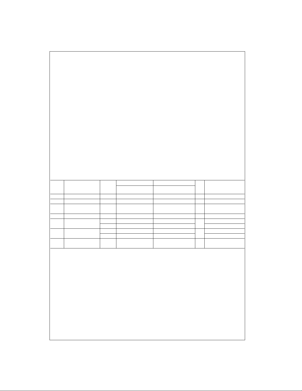
DC Electrical Characteristics
V
Symbol Parameter
V
HIGH Level Input Voltage 2 to 5.5 0.7 V
IH
V
LOW Level Input Voltage 2 to 5.5 0.3 VCCV
IL
I
Control Input
IN
Leakage Current
I
OFF Leakage Current 2 to 5.5 ±0.05 ±10.0 µA0 ≤ A, B ≤ V
OFF
R
Switch On Resistance 4.5 7.2 10 12
ON
(Note 4) 3.0 12 18 12 22 V
On Resistance Flatness 5.0 3.2 3.5 4
R
flat
(Note 4)(Note 6)(Note 7) 3.3 4.5 5 5 IA = −24 mA, VIN = 0.8, 2.5V
I
Quiescent Supply Current 2 to 5.5 1 0.05 10 µAVIN = VCC or GND
CC
Note 4: Measured by the voltage drop between A and B pins at the indicated c urrent through the switch. On Resistanc e is determined by the lower of the
voltages on the two (A or B) pins.
Note 5: All typical values are at the s pec ified V
Note 6: Parameter is characteri z ed but not tested in production.
Note 7: Flatness is defined as the di fference between the ma x im um and minimum value of On Resistanc e ov er the specified rang e of conditions.
CC
(V) Min Typ Max Min Typ
0 to 5.5 ±0.05 ±1.0 µA0 ≤ VIN ≤ 5.5V
, and TA = 25°C.
CC
TA = +25°CT
= −40°C to +85°C
A
(Note 5)
CC
Units Conditions
Max
V
VIN = 2.5V, IIN = 30 mA
Ω
IA = −30 mA, VIN = 1, 2.5, 4V
Ω
I
CC
= 1.5V, IIN = 24 mA
IN
= 0
OUT
NC7SB121
CC
CC
°C/Watt
°C/Watt
3 www.fairchildsemi.com
 Loading...