Fairchild MMBD1701, MMBD1701A, MMBD1703, MMBD1703A, MMBD1704 Schematic [ru]
...
MMBD1701/A / 1703/A / 1704/A / 1705/A
MMBD1701/A / 1703/A / 1704/A / 1705/A
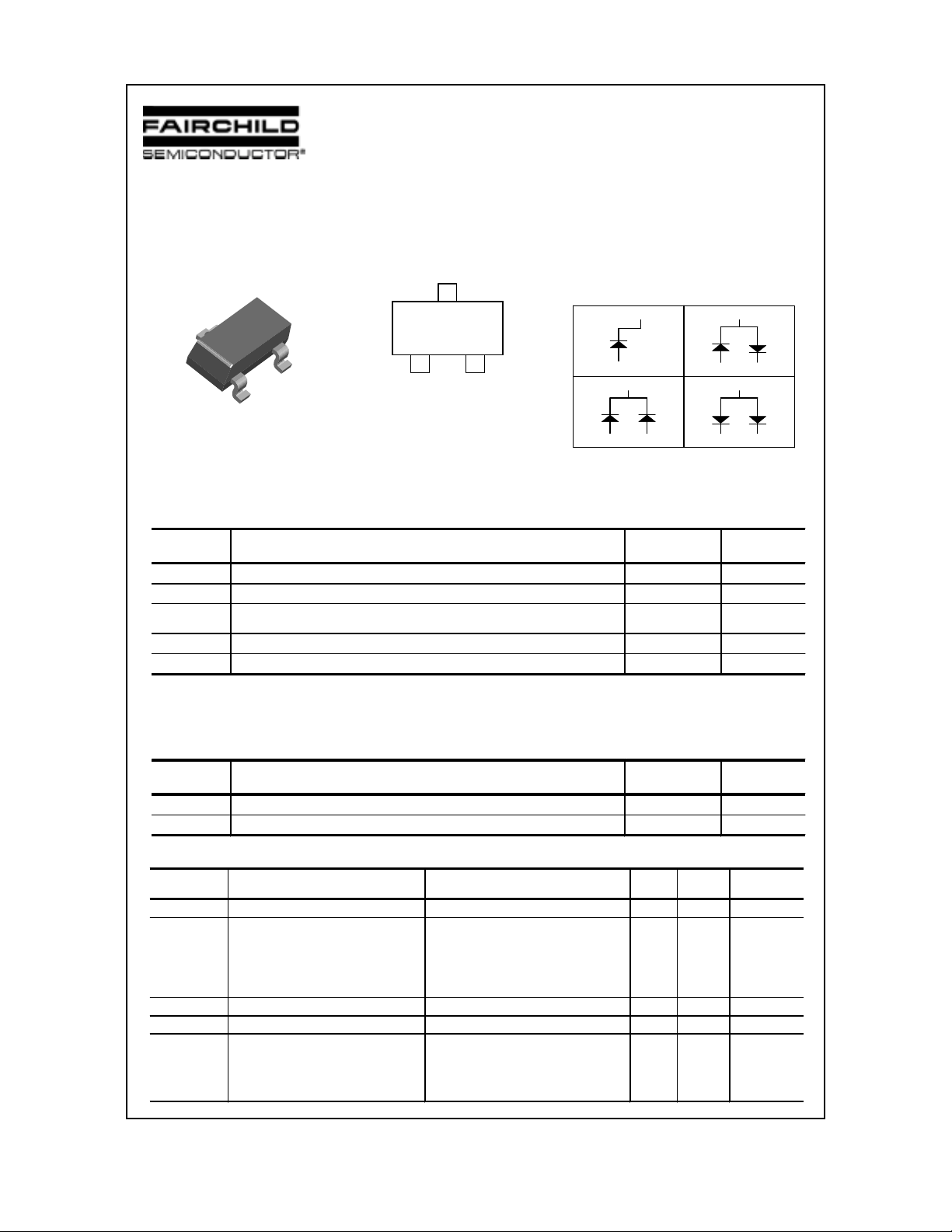
Connection Diagrams
1701
1704 1705
3
2NC
11
3
21
3
1
SOT-23
3
85
2
1
MMBD1701 85 MMBD1701A 85A
MMBD1703 87 MMBD1703A 87A
MMBD1704 88 MMBD1704A 88A
MMBD1705 89 MMBD1705A 89A
2
MARKING
Small Signal Diodes
Absolute Maximum Ratings* T
Symbol
V
Maximum Repetitive Reverse Voltage 30 V
RRM
I
Average Rectified Forward Current 50 mA
F(AV)
I
Non-repetitive Peak Forward Surge Current
FSM
T
stg
TJ
*These ratings are limiting values above which the serviceability of any semiconductor device may be impaired.
NOTES:
1) These ratings are based on a maximum junction temperature of 150 degrees C.
2) These are steady state limits. The factory should be consulted on applications involving pulsed or low duty cycle operations
Storage Temperature Range -55 to +150
Operating Junction Temperature 150
Pulse Width = 1.0 second
Parameter
= 25°C unless otherwise noted
A
Value
250
1
3
1703
2
3
2
Units
mA
°
°
C
C
Thermal Characteristics
Symbol
PD Power Dissipation 350 mW
R
JA
θ
Thermal Resistance, Junction to Ambient 357
Electrical Characteristics T
Symbol
VR Breakdown Voltage
VF Forward Voltage
IR Reverse Current
CT Total Capacitance
trr
2001 Fairchild Semiconductor Corporation
Reverse Recovery Time
Parameter
MMBD1701A-1705A
Parameter
= 25°C unless otherwise noted
MMBD1701-1705
A
Test Conditions
= 5.0 µA
I
R
= 10 µA
I
F
I
= 100 µA
F
IF = 1.0 mA
IF = 10 mA
IF = 20 mA
IF = 50 mA
V
= 20 V 50
R
= 0, f = 1.0 MHz
V
R
I
= IR = 10 mA, I
F
R
= 100 Ω
L
IF = IR = 10 mA, I
= 100 Ω
R
L
= 1.0 mA,
RR
= 1.0 mA,
RR
Value
Min
30
420
520
640
760
810
0.89
Max Units
500
610
740
880
950
1.1
1.0 pF
0.7
1.0
MMBD1700 series, Rev. B1
Units
C/W
°
V
mV
mV
mV
mV
mV
V
nA
ns
ns

T ypical Characteristics
MMBD1701/A / 1703/A / 1704/A / 1705/A
Small Signal Diode
(continued)
60
Ta= 25 C
°
[V]
R
50
Reverse Voltage, V
40
1 2 3 5 10 2 0 3 0 50 100
Revers e C urre n t,I
[uA]
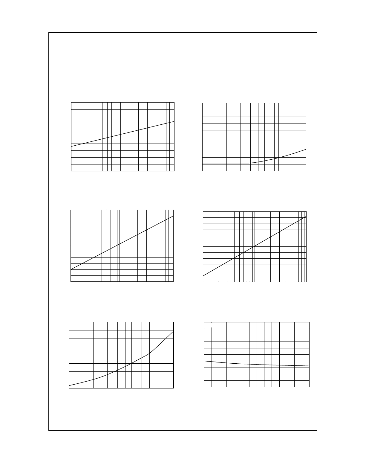
Figure 1. Reverse Voltage vs Reverse Current
BV - 1.0 to 100 uA
600
Ta= 25 C
°
550
[mV]
500
F
450
400
350
Forward Voltage, V
10
Ta= 25 C
°
[nA]
R
5
Reverse Current. I
0
1 2 3 5 10 20
Reverse Voltage, VR [V]
Figure 2. Reverse Current vs Reverse Voltage
IR - 1 to 22V
850
Ta= 25 C
°
800
[mV]
750
F
700
650
600
Forward Voltage, V
300
1 2 3 5 10 20 30 50 100
Forward Current, IF [uA]
Figure 3. Forward V oltage vs Forward Current
VF - 1.0 to 100 uA
1.6
Ta= 25 C
°
1.4
[V]
F
1.2
1.0
Forward Voltage, V
0.8
10 20 30 50 100 200
Forward Current, IF [mA ]
Figure 5. Forward Voltage vs Forward Current
VF - 10 - 200 mA
550
0.1 0.2 0.3 0.5 1 2 3 5 10
Forwa rd C u rren t, IF [mA]
Figure 4. Forward V oltage vs Forward Current
VF - 0.1 to 10 mA
1.0
Ta= 25 C
°
0.9
0.8
0.7
Total Capacitance [pF]
0.6
0.5
0 2 4 6 8 101214
Reverse Voltage [V]
Figure 6. Total Capacitance vs Reverse Current
MMBD1700 series, Rev. B1
 Loading...