查询MM74HC4051MTC供应商
MM74HC4051 • MM74HC4052 • MM74HC4053
8-Channel Analog Multiplexer •
Dual 4-Channel Analog Multiplexer •
Triple 2-Channel Analog Multiplexer
MM74HC4051 • MM74HC4052 • MM74HC4053 8-Channel Analog Multiplexer •
August 1984
Revised May 1999
General Description
The MM74HC4051, MM74HC4052 and MM74HC4053
multiplexers are digitally controlled analog switches implemented in advanced silicon-gate CMOS technology. These
switches have low “on” resista nce and low “off” leakages.
They are bidirectional switches, thus any analog inp ut m ay
be used as an output and vice-versa. Also these switches
contain linearization circuitry which lowers the on resistance and increases switch linearity. These devices allow
control of up to ±6V (peak) ana log signals wi th digital control signals of 0 to 6V. Three supply pins are provided for
, ground, and VEE. This enables the connection of 0–
V
CC
5V logic signals when V
of ±5V when V
inhibit control which when HIGH will disable all switches to
their off state. All analog inputs and outputs and digital
inputs are protected from electrostatic dama ge by diodes
to V
CC
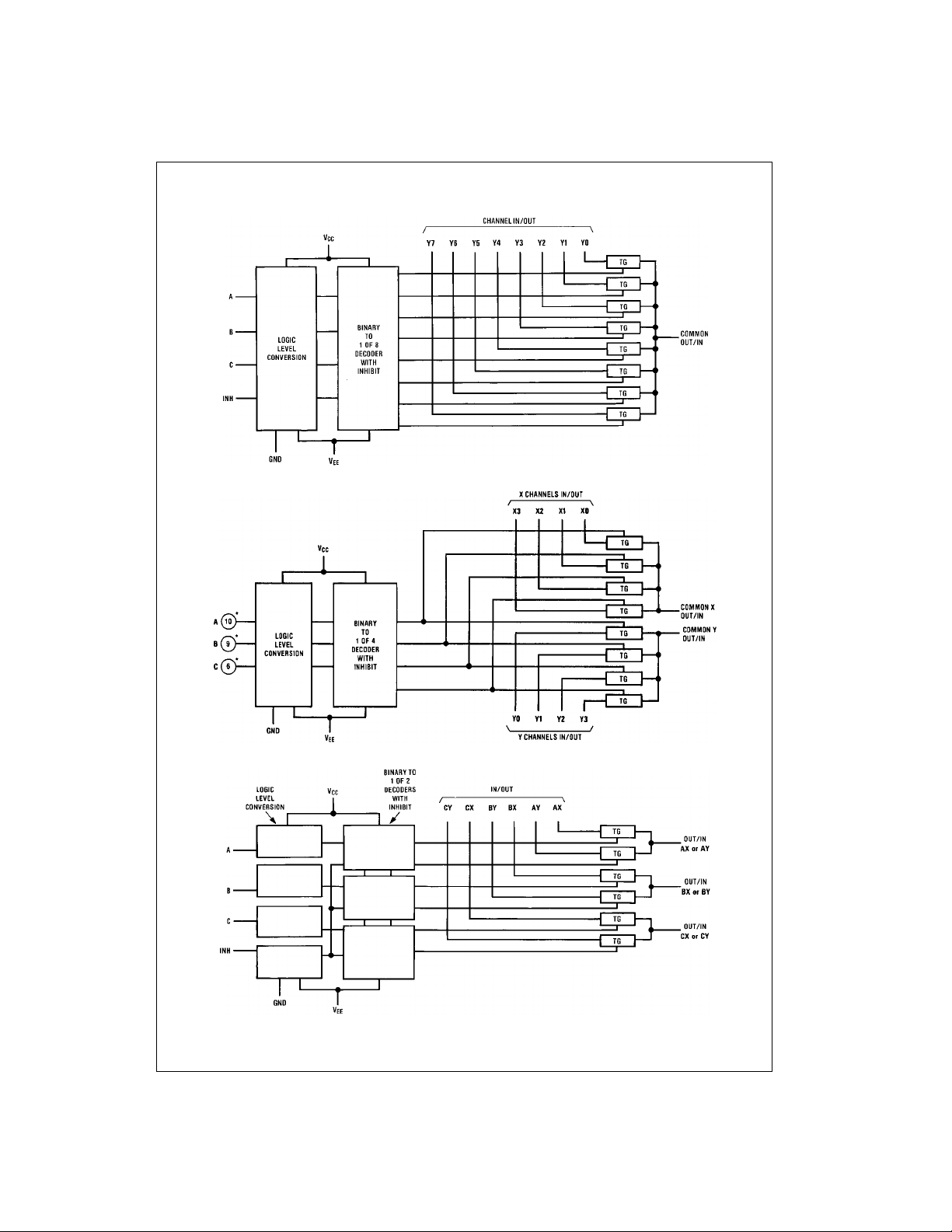
MM74HC4051: This device connects to gether the outp uts
of 8 switches, thus achieving an 8 channel Multiplexer. The
binary code placed on the A , B, and C select lines dete rmines which one o f the eight switches is “on”, and connects one of the eight inputs to the common output.
EE
and ground.
= 5V and an analog input range
CC
= 5V. All three devices also have an
MM74HC4052: This d evice connects t ogether the output s
of 4 switches in two sets, thus achieving a pair of 4-channel
multiplexers. The binary code placed on the A, and B
select lines determine which switch in each 4 channel section is “on”, connecting one of the four inputs in each section to its common output. This enables the implementation
of a 4-channel differential multiplexer.
MM74HC4053: This device contains 6 switches whose outputs are connected together in pairs, thus implementing a
triple 2 channel mult iplexer, or the equivalent of 3 singl epole-double throw con figurations. Each of the A, B, or C
select lines independently controls one pair of switches,
selecting one of the two switches to be “on”.
Features
■ Wide analog input voltage range: ±6V
■ Low “on” resistance:
CC–VEE
CC–VEE
= 4.5V)
= 9V)
50 typ. (V
30 typ. (V
■ Logic level translat ion to enabl e 5V logi c with ±5V ana-
log signals
■ Low quiescent current: 80 µA maximum (74HC)
■ Matched Switch characteristic
Ordering Code:
Order Number Package Number Package Description
MM74HC4051M M16A 16-Lead Small Outline Integrated Circuit (SOIC), JEDEC MS-012, 0.150” Narrow
MM74HC4051WM M16B 16-Lead Small Outline Integrated Circuit (SOIC), JEDEC MS-013, 0.300” Wide
MM74HC4051SJ M16D 16-Lead Small Outline Package (SOP), EIAJ TYPE II, 5.3mm Wide
MM74HC4051MTC MTC16 16-Lead Thin Shrink Small Outline Package (TSSOP), JEDEC MO-153, 4.4mm Wide
MM74HC4051N N16E 16-Lead Plastic Dual-In-Line Package (PDIP), JEDEC MS-0010.300” Wide
MM74HC4052M M16A 16-Lead Small Outline Integrated Circuit (SOIC), JEDEC MS-012, 0.150” Narrow
MM74HC4052WM M16B 16-Lead Small Outline Integrated Circuit (SOIC), JEDEC MS-013, 0.300” Wide
MM74HC4052SJ M16D 16-Lead Small Outline Package (SOP), EIAJ TYPE II, 5.3mm Wide
MM74HC4052MTC MTC16 16-Lead Thin Shrink Small Outline Package (TSSOP), JEDEC MO-153, 4.4mm Wide
MM74HC4052N N16E 16-Lead Plastic Dual-In-Line Package (PDIP), JEDEC MS-0010.300” Wide
MM74HC4053M M16A 16-Lead Small Outline Integrated Circuit (SOIC), JEDEC MS-012, 0.150” Narrow
MM74HC4053WM M16B 16-Lead Small Outline Integrated Circuit (SOIC), JEDEC MS-013, 0.300” Wide
MM74HC4053SJ M16D 16-Lead Small Outline Package (SOP), EIAJ TYPE II, 5.3mm Wide
MM74HC4053MTC MTC16 16-Lead Thin Shrink Small Outline Package (TSSOP), JEDEC MO-153, 4.4mm Wide
MM74HC4053N N16E 16-Lead Plastic Dual-In-Line Package (PDIP), JEDEC MS-0010.300” Wide
Devices also availab le in Tape and Reel. Specify by appending th e s uffix let t er “X” to the ordering code.
© 1999 Fairchild Semiconductor Corporation DS005353.prf www.fairchildsemi.com

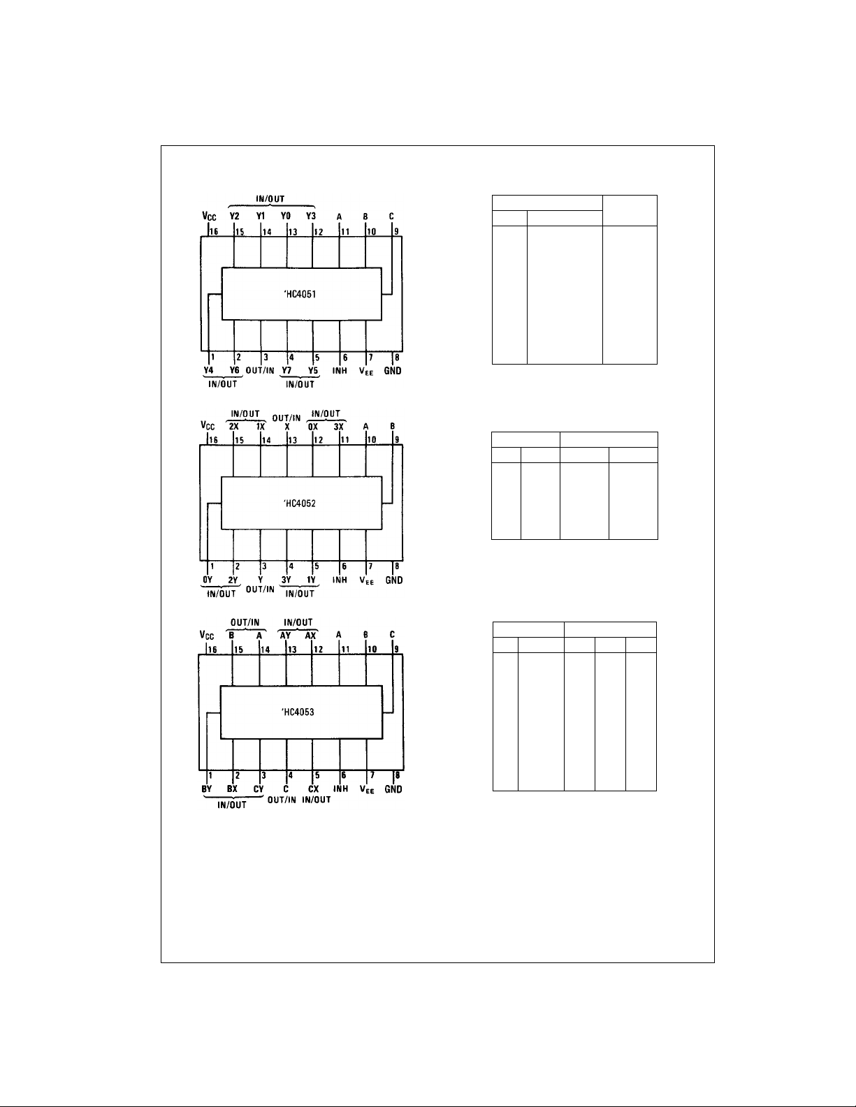
Connection Diagrams
Pin Assignments for DIP, SOIC, SO P and TSSOP
Top View
MM74HC4051 • MM74HC4052 • MM74HC4053
Truth T ables
MM744051
Input “ON”
InhCBAChannel
H XXX None
L LLL Y0
LLLH Y1
LLHL Y2
LLHH Y3
LHLL Y4
LHLH Y5
LHHL Y6
L HHH Y7
MM744052
Inputs “ON” Channels
Inh B A X Y
H X X None None
LLL 0X 0Y
LLH 1X 1Y
LHL 2X 2Y
LHH 3X 3Y
Top View
Top View
www.fairchildsemi.com 2
MM744053
Input “ON” Channels
InhCBA C b a
H X X X None None None
L L L L CX BX AX
LLLHCX BX AY
L L H L CX BY AX
LLHHCX BY AY
L H L L CY BX AX
LHLHCY BX AY
L H H L CY BY AX
L HHH CY BY AY

Logic Diagrams
MM74HC4051 • MM74HC4052 • MM74HC4053
MM74HC4051
MM74HC4052
MM74HC4053
3 www.fairchildsemi.com

Absolute Maximum Ratings(Note 1)
(Note 2)
Supply Voltage (V
Supply Voltage (V
Control Input Voltage (V
Switch I/O Voltage (V
Clamp Diode Current (I
Output Current, per pin (I
or GND Current, per pin (ICC) ±50 mA
V
CC
Storage Temperature Range (T
Power Dissipation (P
) −0.5 to +7.5V
CC
) +0.5 to −7.5V
EE
) −1.5 to V
IN
)V
IO
, IOK) ±20 mA
IK
) ±25 mA
OUT
STG
)
D
−0.5 to V
EE
) −65°C to +150°C
(Note 3) 600 mW
S.O. Package only 500 mW
Lead Temperature (T
)
L
(Soldering 10 seconds) 260°C
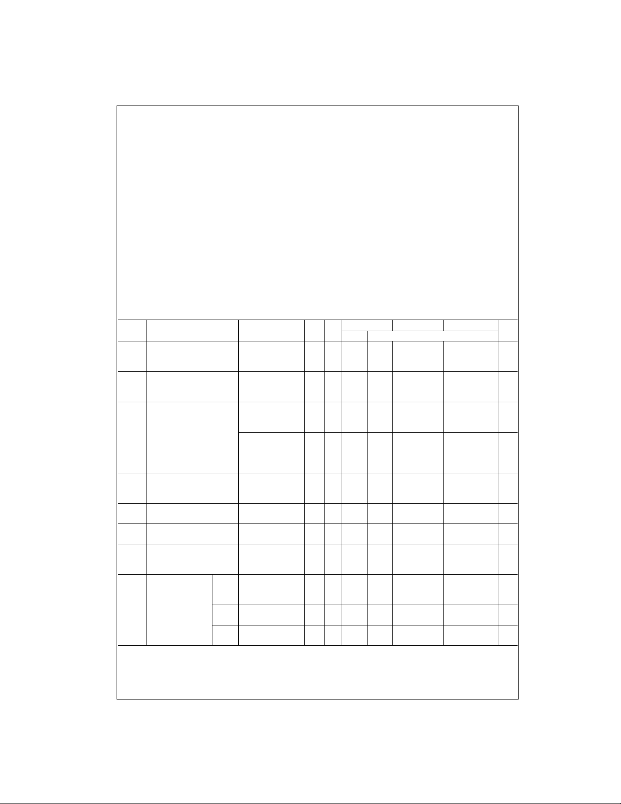
DC Electrical Characteristics (Note 4)
Symbol Parameter Conditions
MM74HC4051 • MM74HC4052 • MM74HC4053
V
Minimum HIGH Level 2.0V 1.5 1.5 1.5 V
IH
Input Voltage 4.5V 3.15 3.15 3.15 V
V
Maximum LOW Level 2.0V 0.5 0.5 0.5 V
IL
Input Voltage 4.5V 1.35 1.35 1.35 V
R
Maximum “ON” Resistance V
ON
(Note 5) V
R
Maximum “ON” Resistance V
ON
Matching V
I
Maximum Control V
IN
Input Current V
I
Maximum Quiescent V
CC
Supply Current I
I
Maximum Switch “OFF” V
IZ
Leakage Current V
(Switch Input) V
I
Maximum Switch V
IZ
“ON” Leakage HC4051 V
Current (Figure 3)
HC4052 V
HC4053 V
= VIL, IS = 2.0 mA GND 4.5V 40 160 200 240 Ω
INH
= VCC to V
IS
(Figure 1) −6.0V 6.0V 20 100 125 140 Ω
V
= VIL, IS = 2.0 mA GND 2.0V 100 230 280 320 Ω
INH
V
= VCC or V
IS
(Figure 1) −4.5V 4.5V 20 90 120 140 Ω
= V
CTL
IL
= VCC to GND −4.5V 4.5V 5 10 15 15 Ω
IS
= VCCor GND ±0.1 ±1.0 ±1.0 µA
IN
= 2−6V
CC
= VCC or GND GND 6.0V 8 80 160 µA
IN
= 0 µA −6.0V 6.0V 16 160 320 µA
OUT
= VCCor V
OS
= VEEor V
IS
= VIH (Figure 2)
INH
= VCC to V
IS
= V
INH
IL
V
= VCC to V
IS
= V
(Figure 3) −6.0V 6.0V ±0.2 ±2.0 ±2.0 µA
INH
IL
V
= VCC to V
IS
= VIL (Figure 3) −6.0V 6.0V ±0.1 ±1.0 ±1.0 µA
INH
Recommended Operating
Conditions
Min Max Units
Supply Voltage (V
+1.5V
CC
CC
Supply Voltage (V
+0.5V
DC Input or Output Voltage
, V
(V
IN
OUT
Operating Temperature Range (T
Input Rise or Fall Times
, tf) VCC = 2.0V 1000 ns
(t
r
V
CC
V
Note 1: Absolute Maximum Ratings are those values beyond which damage to the device may occur.
Note 2: Unless otherwise specified all voltages are referenced to ground.
Note 3: Power Dissipation tem perature de rating — pla stic “N” pac kage: −
12 mW/°C from 65 °C to 85°C.
VEEV
−4.5V 4.5V 30 120 150 170 Ω
EE
GND 4.5V 40 110 140 170 Ω
EE
−6.0V 6.0V 15 80 100 115 Ω
GND 4.5V 10 20 25 25 Ω
−6.0V 6.0V 5 10 12 15 Ω
GND 6.0V ±60 ±600 ±600 nA
EE
−6.0V 6.0V ±100 ±1000 ±1000 nA
CC
GND 6.0V ±0.2 ±2.0 ±2.0 µA
EE
−6.0V 6.0V ±0.4 ±4.0 ±4.0 µA
GND 6.0V ±0.1 ±1.0 ±1.0 µA
EE
GND 6.0V ±0.1 ±1.0 ±1.0 µA
EE
CC
TA = 25°CTA = −40 to 85°CTA = −55 to 125°C
CC
Typ Guaranteed Limits
6.0V 4.2 4.2 4.2 V
6.0V 1.8 1.8 1.8 V
)26V
CC
)0−6V
EE
)0V
) −40 +85 °C
A
= 4.5V 500 ns
= 6.0V 400 ns
CC
V
Units
www.fairchildsemi.com 4
 Loading...