

February 1984
Revised September 2001
MM74HC4020 • MM74HC4040
14-Stage Binary Counter • 12-Stage Binary Counter
MM74HC4020 • MM74HC4040 14-Stage Binary Counter • 12-Stage Binary Counter
General Description
The MM74HC4020 , MM74HC4040 , are high speed binary
ripple carry count ers . T hes e co unters are impleme nte d u ti lizing advanced silicon- gate CMOS technology to ach ieve
speed performance similar to LS-TTL logic while retaining
the low power and high noise immunity of CMOS.
The MM74HC4020 is a 14 stage counter and the
MM74HC4040 is a 12-stage counter. Both devices are
incremented on the falling edge (negative transition) of the
input clock, and all th eir outp uts ar e reset to a l ow leve l by
applying a logical high on their reset input.
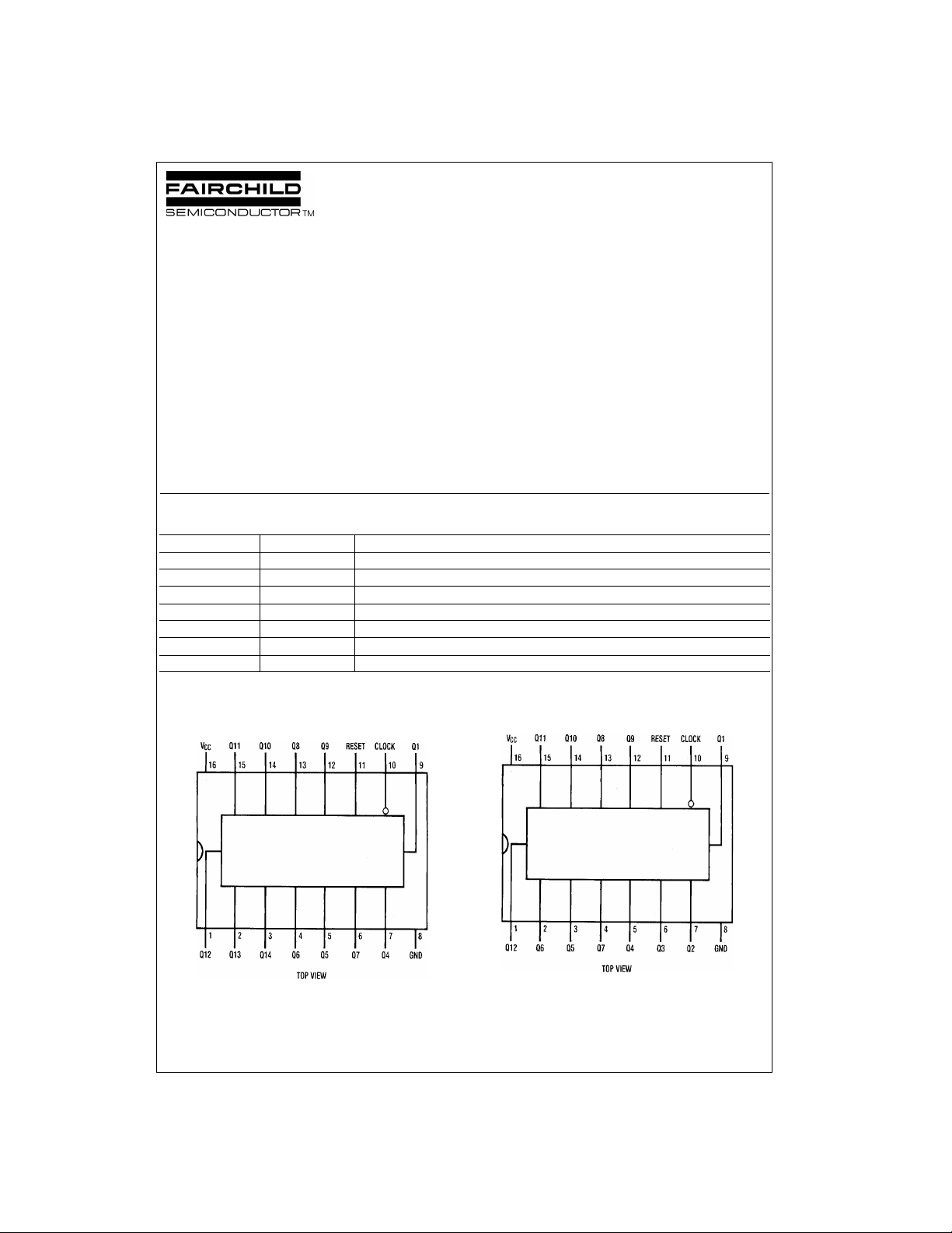
These devices are pin equivalent to the CD4020 and
CD4040 respectively. All inputs are protected from damage
due to static discharge by protection diodes to V
ground.
CC
and
Features
■ Typical propagation delay: 16 ns
■ Wide operating voltage ran ge: 2–6V
■ Low input current: 1
■ Low quiescent current: 80
■ Output drive capability: 10 LS-TTL loads
µA maximum
µA maximum (74HC Series)
Ordering Code:
Order Number Package Number Package Description
MM74HC4020M M16A 16-Lead Small Outline Integrated Circuit (SOIC), JEDEC MS-012, 0.150" Narrow
MM74HC4020SJ M16D 16-Lead Small Outline Package (SOP), EIAJ TYPE II, 5.3mm Wide
MM74HC4020N N16E 16-Lead Plastic Dual-In-Line Package (PDIP), JEDEC MS-001, 0.300" Wide
MM74HC4040M M16A 16-Lead Small Outline Integrated Circuit (SOIC), JEDEC MS-012, 0.150" Narrow
MM74HC4040SJ M16D 16-Lead Small Outline Package (SOP), EIAJ TYPE II, 5.3mm Wide
MM74HC4040MTC MTC16 16-Lead Thin Shrink Small Outline Package (TSSOP), JEDEC MO-153, 4.4mm Wide
MM74HC4040N N16E 16-Lead Plastic Dual-In-Line Package (PDIP), JEDEC MS-001, 0.300" Wide
Devices also availab l e in Tape and Reel. Specify by appending th e s uffix let t er “X” to the ordering code.
Connection Diagrams
MM74HC4020
© 2001 Fairchild Semiconductor Corporation DS005216 www.fairchildsemi.com
MM74HC4040
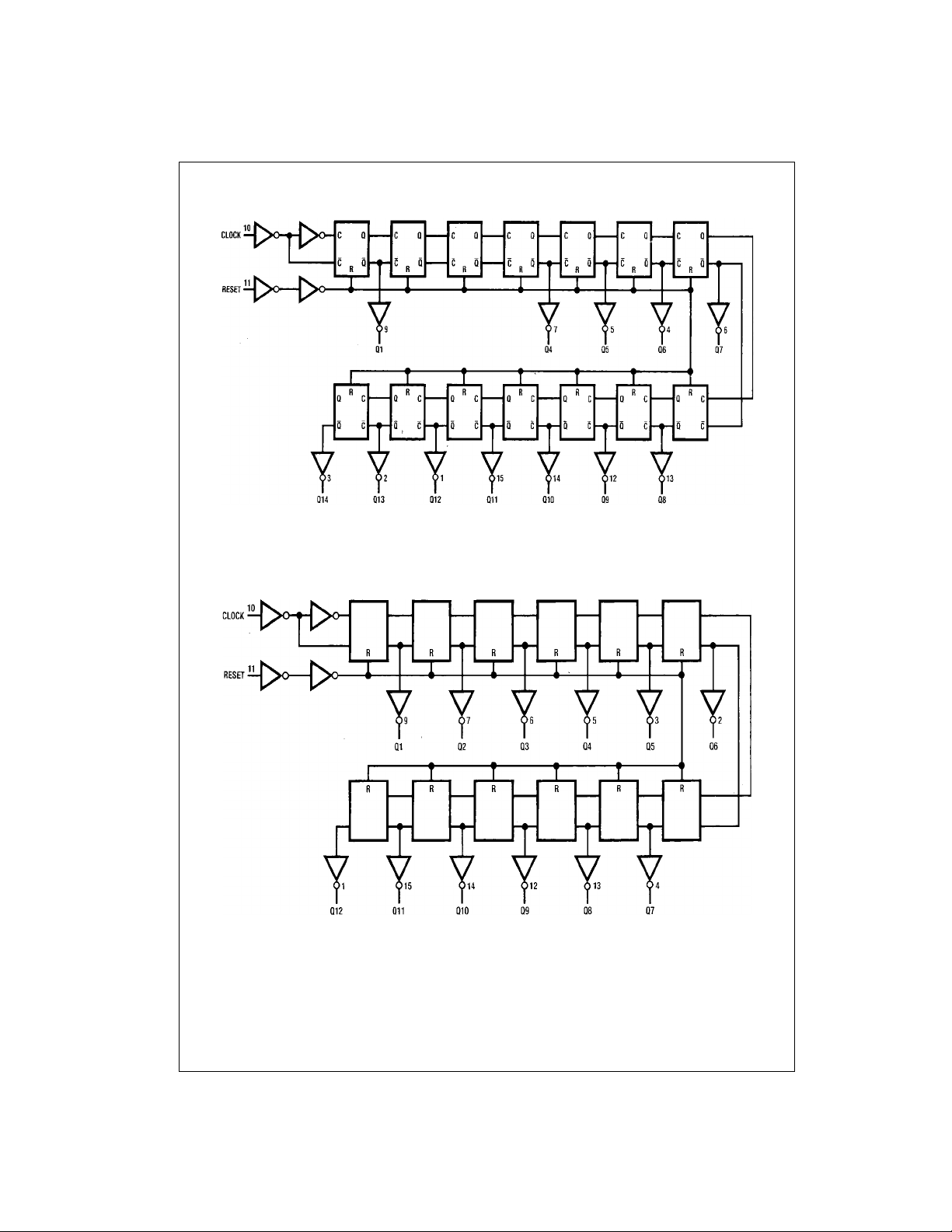
Logic Diagrams
MM74HC4020 • MM74HC4040
MM74HC4020
MM74HC4040
www.fairchildsemi.com 2
Absolute Maximum Ratings(Note 1)
(Note 2)
Supply Voltage (VCC) −0.5 to +7.0V
DC Input Voltage (V
DC Output Voltage (V
Clamp Diode Current (I
DC Output Current, per pin (I
DC V
or GND Current, per pin (ICC) ±50 mA
CC
Storage Temperature Range (T
Power Dissipation (P
(Note 3) 600 mW
S.O. Package only 500 mW
Lead Temperature (T
(Soldering 10 seconds) 260
) −1.5 to V
IN
) −0.5 to V
OUT
) ±20 mA
CD
) ±25 mA
OUT
) −65°C to +150°C
STG
)
D
)
L
CC
CC
Recommended Operating
Conditions
+1.5V
Supply Voltage (V
+0.5V
DC Input or Output Voltage 0 V
, V
(V
IN
OUT
Operating Temperature Range (T
Input Rise or Fall Times
, tf) V
(t
r
CC
V
CC
V
Note 1: Maximum Ratings are those v alues beyo nd which damage to t he
device may occur.
Note 2: Unless otherwise specified all voltages are referenced to ground.
°C
Note 3: Power Dissipation te mperature d erating — pl astic “N” package: −
12 mW/°C from 65°C to 85°C.
CC
)26V
CC
)
) −40 +85 °C
A
= 2.0V 1000 ns
= 4.5V 500 ns
= 6.0V 400 ns
Min Max Units
CC
DC Electrical Characteristics (Note 4)
Symbol Parameter Conditions
V
V
V
V
I
I
Minimum HIGH Level Input 2.0V 1.5 1.5 1.5 V
IH
Voltage 4.5V 3.15 3.15 3.15 V
Maximum LOW Level Input 2.0V 0.5 0.5 0.5 V
IL
Voltage 4.5V 1.35 1.35 1.35 V
Minimum HIGH Level Output V
OH
Voltage |I
Maximum LOW Level Output V
OL
Voltage |I
Maximum Input Current V
IN
Maximum Quiescent Supply V
CC
Current I
Note 4: For a power supply of 5V ±10% the worst case output voltages (VOH, and VOL) occur for HC at 4.5V. Thus the 4. 5V valu es shou ld be u sed when
designing with this supply. Worst case V
, ICC, and IOZ) occur for CMOS at the higher voltage and so th e 6. 0V values should be used.
rent (I
IN
= VIH or V
IN
OUT
V
IN
|I
OUT
|I
OUT
IN
OUT
V
IN
|I
OUT
|I
OUT
IN
IN
OUT
and VIL occur at V
IH
IL
| ≤ 20 µA 2.0V 2.0 1.9 1.9 1.9 V
= VIH or V
IL
| ≤ 4.0 mA 4.5V 4.2 3.98 3.84 3.7 V
| ≤ 5.2 mA 6.0V 5.7 5.48 5.34 5.2 V
= VIH or V
IL
| ≤ 20 µA 2.0V 0 0.1 0.1 0.1 V
= VIH or V
IL
| ≤ 4.0 mA 4.5V 0.2 .26 0.33 0.4 V
| ≤ 5.2 mA 6.0V 0.2 .26 0.33 0.4 V
= VCC or GND 6.0V ±0.1 ±1.0 ±1.0 µA
= VCC or GND 6.0V 8.0 80 160 µA
= 0 µA
= 5.5V and 4.5V respectively. (The VIH value at 5.5V is 3.85V.) The worst case leakage cur-
CC
V
6.0V 4.2 4.2 4.2 V
6.0V 1.8 1.8 1.8 V
4.5V 4.5 4 .4 4.4 4.4 V
6.0V 6.0 5 .9 5.9 5.9 V
4.5V 0 0.1 0.1 0.1 V
6.0V 0 0.1 0.1 0.1 V
TA = 25°CTA = −40 to 85°CTA = −55 to 125°C
CC
Typ Guaranteed Limits
MM74HC4020 • MM74HC4040
V
Units
3 www.fairchildsemi.com
 Loading...