

Fairchild MM74HC174 service manual

MM74HC174
Hex D-Type Flip-Flops with Clear
MM74HC174 Hex D-Type Flip-Flops with Clear
September 1983
Revised February 1999
General Description
The MM74HC174 edge triggered flip-flops utilize advanced
silicon-gate CMOS technology to implement D-type flipflops. They possess high no ise immunity, low power, and
speeds comparable to low power Schottky TTL circuits.
This device contains 6 master-slave flip- flops with a common clock and common clear. Data on the D in put having
the specified setup and hold times is transferred to th e Q
output on the LOW-to-HIGH transition of the CLOCK input.
The CLEAR input when LOW, sets all outputs to a low
state.
Each output can drive 10 low p ower Sch ottky TTL eq uivalent loads. The MM74HC174 is functionally as well as pin
compatible to the 74L S174. All inputs are protected fr om
damage due to static discharge by diodes to V
ground.
CC
and
Features
■ Typical propagation delay: 16 ns
■ Wide operating voltage ran ge: 2–6V
■ Low input current: 1 µA maximum
■ Low quiescent current: 80 µA (74HC Series)
■ Output drive: 10 LSTTL loads
Ordering Code:
Order Number Package Number Package Description
MM74HC174M M16A 16-Lead Small Outline Integrated Circuit (SOIC), JEDEC MS-012, 0.150” Narrow
MM74HC174SJ M16D 16-Lead Small Outline Package (SOP), EIAJ TYPE II, 5.3mm Wide
MM74HC174MTC MTC16 16-Lead Thin Shrink Small Outline Package (TSSOP), JEDEC MO-153, 4.4mm Wide
MM74HC174N N16E 16-Lead Plastic Dual-In-Line Package (PDIP), JEDEC MS-001, 0.300” Wide
Devices also availab le in Tape and Reel. Specify by appending th e s uffix let t er “X” to the ordering code.
Connection Diagram
Pin Assignments for DIP, SOIC, SOP and TSSOP
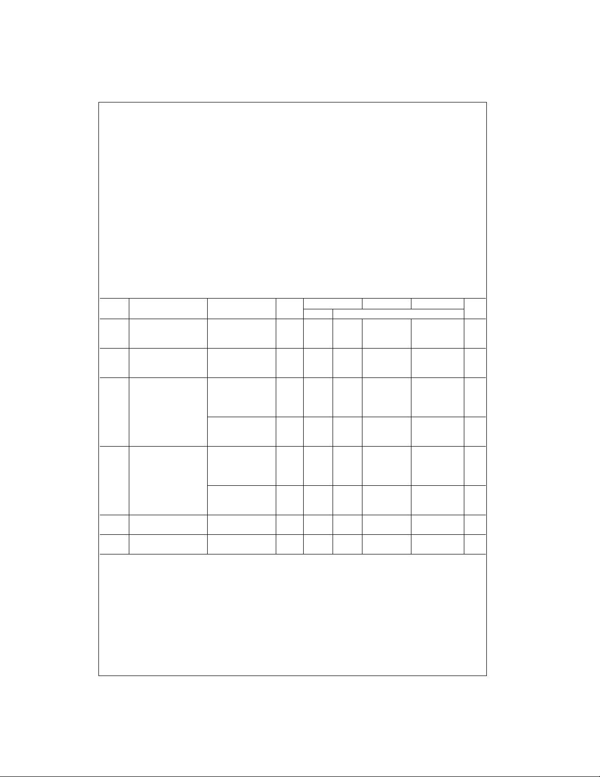
Truth Table
(Each Flip-Flop)
Inputs Outputs
Clear Clock D Q
LXXL
H ↑ HH
H ↑ LL
HLXQ
H = HIGH Level (steady state)
L = LOW Level (steady state)
X = Don't Care
↑ = Transition from LOW-to-HIGH level
= The level of Q before the indic ated steady stat e input conditions were
Q
0
established.
0
© 1999 Fairchild Semiconductor Corporation DS005318.prf www.fairchildsemi.com
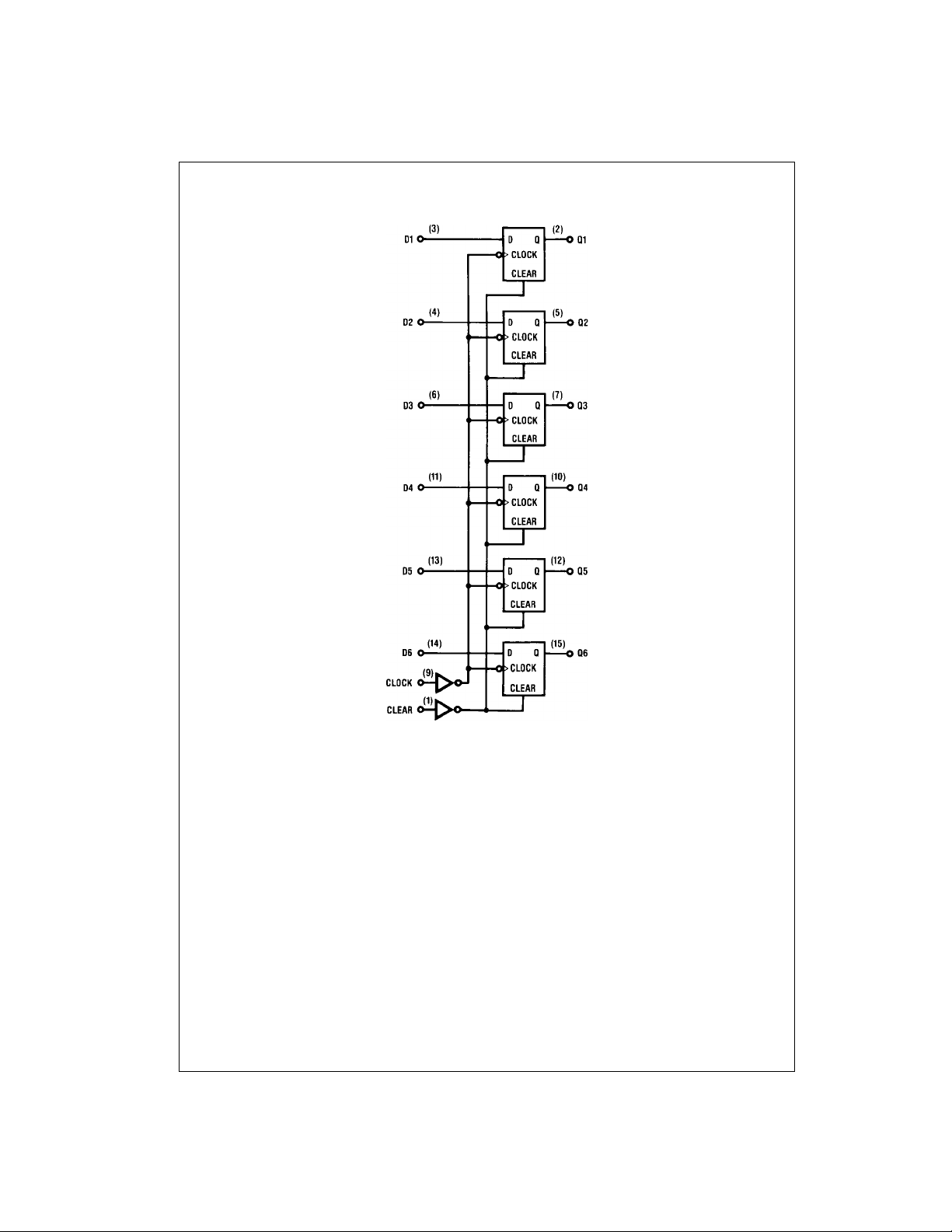
Logic Diagram
MM74HC174
www.fairchildsemi.com 2
Absolute Maximum Ratings(Note 1)
(Note 2)
Supply Voltage (VCC) −0.5 to +7.0V
DC Input Voltage (V
DC Output Voltage (V
Clamp Diode Current (I
DC Output Current, per pin (I
or GND Current, per pin (ICC) ±50 mA
DC V
CC
Storage Temperature Range (T
Power Dissipation (P
(Note 3) 600 mW
S.O. Package only 500 mW
Lead Temperature (T
(Soldering 10 seconds ) 260°C
) −1.5 to V
IN
) −0.5 to V
OUT
, IOK) ±20 mA
IK
) ±25 mA
OUT
) −65°C to +150°C
STG
)
D
)
L
CC
CC
Recommended Operating
Conditions
+1.5V
+0.5V
Supply Voltage (V
)26V
CC
DC Input or Output Voltage
, V
(V
Operating Temperature Range (T
)0V
IN
OUT
) −40 +85 °C
A
Input Rise or Fall Times
, tf) V
(t
Note 1: Absolute Maximum Ra tings are those valu es beyond w hich damage to the device may occur.
Note 2: Unless otherwise specified all voltages are referenced to ground.
Note 3: Power Dissipation te mperature d erating — pl astic “N” pa ckage: −
12 mW/°C from 65°C to 85°C.
= 2.0V 1000 ns
r
CC
= 4.5V 500 ns
V
CC
= 6.0V 400 ns
V
CC
Min Max Units
CC
DC Electrical Characteristics (Note 4)
Symbol Parameter Conditions
V
V
V
V
I
I
Minimum HIGH Level 2.0V 1.5 1.5 1.5 V
IH
Input Voltage 4.5V 3.15 3.15 3.15 V
Maximum LOW Level 2.0V 0.5 0.5 0.5 V
IL
Input Voltage 4.5V 1.35 1.35 1.35 V
Minimum HIGH Level V
OH
Output Voltage |I
Maximum LOW Level V
OL
Output Voltage |I
Maximum Input V
IN
Current
Maximum Quiescent V
CC
Supply Current I
Note 4: For a powe r supply o f 5V ±10% the worst case output voltages (VOH, and VOL) occur for HC at 4.5V. Thus the 4. 5V valu es shou ld be u sed when
designing with this supply. Worst case V
, ICC, and IOZ) occur for CMOS at the higher voltage and so th e 6. 0V values should be us ed.
rent (I
IN
= VIH or V
IN
OUT
V
IN
|I
OUT
|I
OUT
IN
OUT
V
IN
|I
OUT
|I
OUT
IN
IN
OUT
and VIL occur at V
IH
IL
| ≤ 20 µA 2.0V 2.0 1.9 1.9 1.9 V
= VIH or V
IL
| ≤ 4.0 mA 4.5V 4.2 3.98 3.84 3.7 V
| ≤ 5.2 mA 6.0V 5.7 5.48 5.34 5.2 V
= VIH or V
IL
| ≤ 20 µA 2.0V 0 0.1 0.1 0.1 V
= VIH or V
IL
| ≤ 4.0 mA 4.5V 0.2 0.26 0.33 0.4 V
| ≤ 5.2 mA 6.0V 0.2 0.26 0.33 0.4 V
= VCC or GND 6.0V ±0.1 ±1.0 ±1.0 µA
= VCC or GND 6.0V 8.0 80 160 µA
= 0 µA
CC
V
CC
6.0V 4.2 4.2 4.2 V
6.0V 1.8 1.8 1.8 V
4.5V 4.5 4.4 4.4 4.4 V
6.0V 6.0 5.9 5.9 5.9 V
4.5V 0 0.1 0.1 0.1 V
6.0V 0 0.1 0.1 0.1 V
= 5.5V and 4.5V respectively. (The VIH value at 5.5V is 3 .8 5V.) The worst c as e leakage cur-
TA = 25°CTA = −40 to 85°CTA = −55 to 125°C
Typ Guaranteed Limits
MM74HC174
V
Units
3 www.fairchildsemi.com
 Loading...