

MM74HC00 — Quad 2-Input NAND Gate
February 2008
MM74HC00
Quad 2-Input NAND Gate
Features
■
Typical propagation delay: 8ns
Wide power supply range: 2V–6V
■
■
Low quiescent current: 20µA maximum (74HC Series)
Low input current: 1µA maximum
■
■
Fanout of 10 LS-TTL loads
General Description
The MM74HC00 NAND gates utilize advanced silicongate CMOS technology to achieve operating speeds
similar to LS-TTL gates with the low power consumption
of standard CMOS integrated circuits. All gates have
buffered outputs. All devices have high noise immunity
and the ability to drive 10 LS-TTL loads. The 74HC logic
family is functionally as well as pin-out compatible with
the standard 74LS logic family. All inputs are protected
from damage due to static discharge by internal diode
clamps to V
and ground.
CC
Ordering Information
Package
Order Number
MM74HC00M M14A 14-Lead Small Outline Integrated Circuit (SOIC), JEDEC MS-012, 0.150" Narrow
MM74HC00SJ M14D 14-Lead Small Outline Package (SOP), EIAJ TYPE II, 5.3mm Wide
MM74HC00MTC MTC14 14-Lead Thin Shrink Small Outline Package (TSSOP), JEDEC MO-153, 4.4mm Wide
MM74HC00N N14A 14-Lead Plastic Dual-In-Line Package (PDIP), JEDEC MS-001, 0.300" Wide
Device also available in Tape and Reel. Specify by appending suffix letter “X” to the ordering number.
All packages are lead free per JEDEC: J-STD-020B standard.
Number Package Description
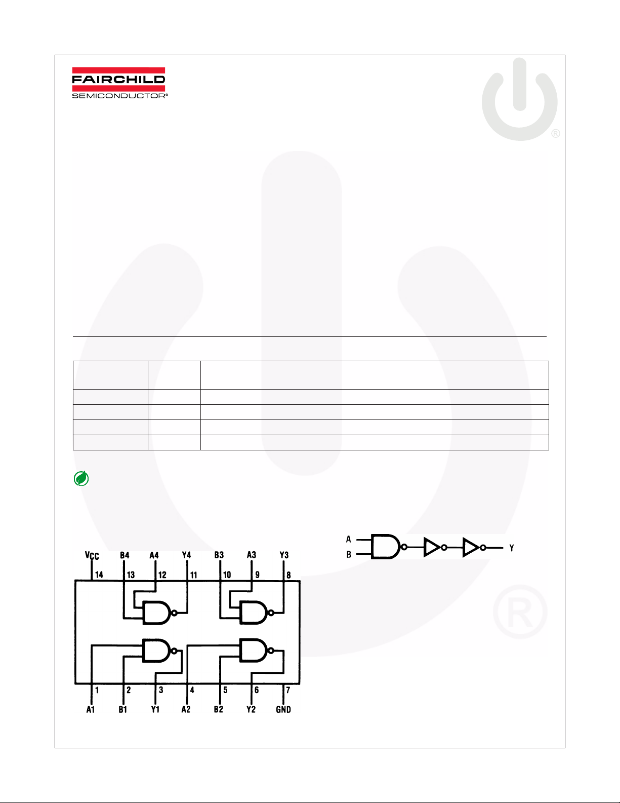
Connection Diagram
Pin Assignments for DIP, SOIC, SOP and TSSOP
Top View
©1983 Fairchild Semiconductor Corporation www.fairchildsemi.com
MM74HC00 Rev. 1.3.0
Logic Diagram
=
=
=
MM74HC00 — Quad 2-Input NAND Gate
Absolute Maximum Ratings
(1)
Stresses exceeding the absolute maximum ratings may damage the device. The device may not function or be
operable above the recommended operating conditions and stressing the parts to these levels is not recommended.
In addition, extended exposure to stresses above the recommended operating conditions may affect device reliability.
The absolute maximum ratings are stress ratings only.
Symbol Parameter Rating
V
CC
V
IN
V
OUT
, I
I
IK
I
OUT
I
CC
T
STG
P
D
T
Notes:
1. Unless otherwise specified all voltages are referenced to ground.
2. Power Dissipation temperature derating — plastic “N” package: –12mW/°C from 65°C to 85°C.
Supply Voltage –0.5 to +7.0V
DC Input Voltage –1.5 to V
DC Output Voltage –0.5 to V
Clamp Diode Current ±20mA
OK
DC Output Current, per pin ±25mA
DC V
or GND Current, per pin ±50mA
CC
Storage Temperature Range –65°C to +150°C
Power Dissipation
Note 2 600mW
S.O. Package only 500mW
Lead Temperature (Soldering 10 seconds) 260°C
L
CC
CC
+1.5V
+0.5V
Recommended Operating Conditions
The Recommended Operating Conditions table defines the conditions for actual device operation. Recommended
operating conditions are specified to ensure optimal performance to the datasheet specifications. Fairchild does not
recommend exceeding them or designing to absolute maximum ratings.
Symbol Parameter Min. Max. Units
V
CC
V
, V
IN
T
A
t
, t
r
Supply Voltage 2 6 V
DC Input or Output Voltage 0 V
OUT
Operating Temperature Range –40 +85 °C
Input Rise or Fall Times
f
V
V
V
2.0V
CC
4.5V 500 ns
CC
6.0V 400 ns
CC
CC
1000 ns
V
©1983 Fairchild Semiconductor Corporation www.fairchildsemi.com
MM74HC00 Rev. 1.3.0 2
=
=
=
=
=
| ≤
=
| ≤
=
| ≤
=
| ≤
=
| ≤
=
| ≤
=
=
=
MM74HC00 — Quad 2-Input NAND Gate
DC Electrical Characteristics
Symbol Parameter V
V
Minimum HIGH Level
IH
Input Voltage
(3)
(V) Conditions
CC
2.0 1.5 1.5 1.5 V
4.5 3.15 3.15 3.15
6.0 4.2 4.2 4.2
V
Maximum LOW Level
IL
Input Voltage
2.0 0.5 0.5 0.5 V
4.5 1.35 1.35 1.35
6.0 1.8 1.8 1.8
V
Minimum HIGH Level
OH
Output Voltage
2.0 V
4.5 4.5 4.4 4.4 4.4
|I
IN
OUT
V
or V
IH
20µA
,
IL
6.0 6.0 5.9 5.9 5.9
V
or V
4.0mA
or V
5.2mA
,
20µA
,
IL
,
IL
4.5 V
6.0 V
V
Maximum LOW Level
OL
Output Voltage
2.0 V
4.5 0 0.1 0.1 0.1
|I
|I
|I
IN
OUT
IN
OUT
IN
OUT
IH
V
IH
V
IH
6.0 0 0.1 0.1 0.1
V
IN
IN
IN
,
IH
4.0mA
V
,
IH
5.2mA
V
or GND ±0.1 ±1.0 ±1.0 µA
CC
I
IN
Maximum Input
4.5 V
6.0 V
6.0 V
|I
|I
OUT
OUT
Current
I
Maximum Quiescent
CC
Supply Current
6.0 V
IN
I
OUT
V
0µA
or GND,
CC
Note:
3. For a power supply of 5V ±10% the worst case output voltages (V
values should be used when designing with this supply. Worst case V
respectively. (The V
value at 5.5V is 3.85V.) The worst case leakage current (I
IH
the higher voltage and so the 6.0V values should be used.
T
–40°C
T
25°C
A
A
to 85°C
T
–55°C
A
to 125°C
UnitsTyp. Guaranteed Limits
2.0 1.9 1.9 1.9 V
4.2 3.98 3.84 3.7
5.7 5.48 5.34 5.2
0 0.1 0.1 0.1 V
0.2 0.26 0.33 0.4
0.2 0.26 0.33 0.4
2.0 20 40 µA
OH
, and V
IH
) occur for HC at 4.5V. Thus the 4.5V
OL
and V
occur at V
IL
, I
IN
CC
, and I
5.5V and 4.5V
CC
) occur for CMOS at
OZ
©1983 Fairchild Semiconductor Corporation www.fairchildsemi.com
MM74HC00 Rev. 1.3.0 3
 Loading...