Fairchild MM74C925, MM74C926, MM74C927, MM74C928 service manual

查询74C925供应商
MM74C925 • MM74C926 • MM74C927 • MM74C928
4-Digit Counters with Multiplexed
7-Segment Output Drivers
MM74C925 • MM74C926 • MM74C927 • MM74C928 4-Digit Counters with Multiplexed 7-Segment Output Drivers
October 1987
Revised January 1999
General Description
The MM74C925, MM74C 9 26, M M74 C92 7 and MM7 4C 9 28
CMOS counters consist of a 4-digit counter, an internal output latch, NPN output sourcing drivers for a 7-segment display, and an internal multiplexing circuitry with four
multiplexing outputs. The multiplexing circuit has its own
free-running oscillator, and requires no external clock. The
counters advance on negative edge of clock. A HIGH signal on the Reset input will reset the counter to zero, and
reset the carry-out LOW. A LOW signal on the Latch
Enable input will latch the number in the counters into the
internal output latches. A HIGH signal on Disp lay Select
input will select the number in the coun ter to be displ ayed;
a LOW level signal on the Display Select will select the
number in the output latch to be displayed.
The MM74C925 is a 4-decade counter and has Latch
Enable, Clock and Reset inputs.
The MM74C926 is like the MM74C9 25 except that it ha s a
display select and a carry-out used for cascading counters.
The carry-out sig nal goes HIGH at 6000 , goes back LOW
at 0000.
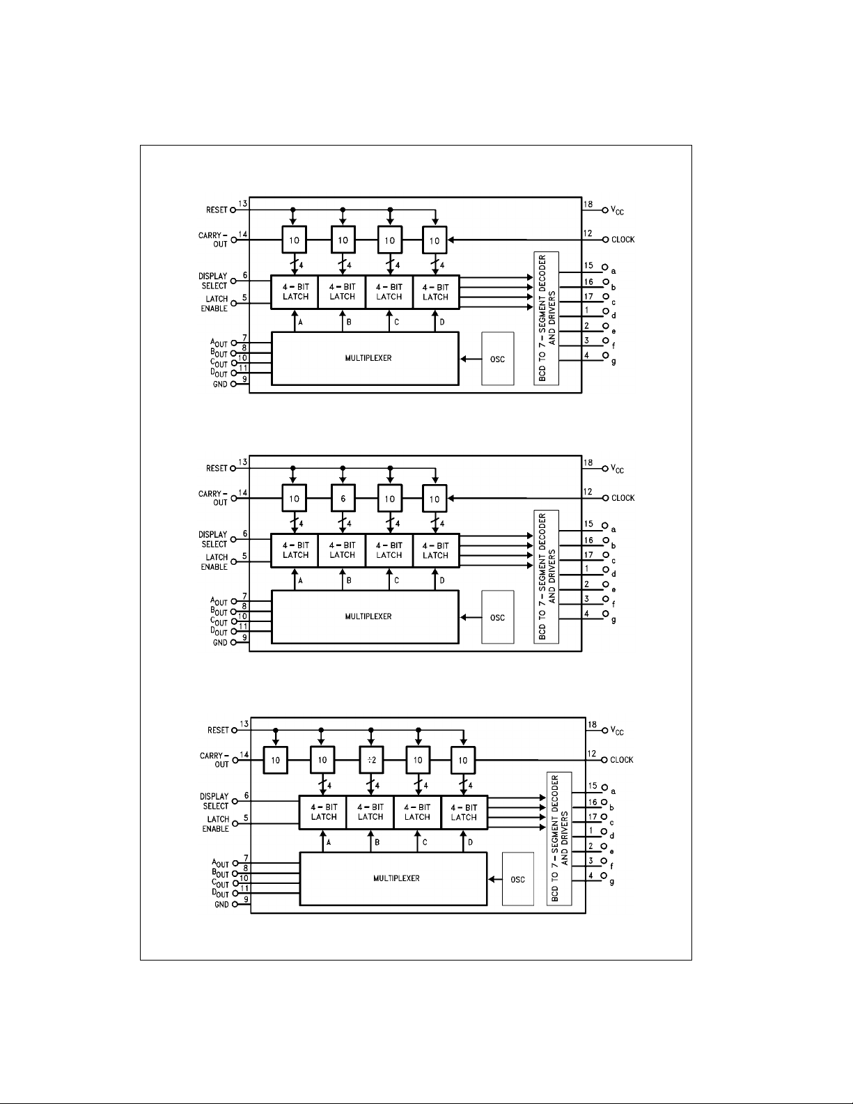
The MM74C927 is like the M M74C926 except the second
most significant digi t divides by 6 rather than 10. Thu s, if
the clock input frequency is 10 Hz, the display would read
tenths of seconds and minutes (i.e., 9:59.9).
The MM74C928 is like the MM74C926 except the most significant digit divides by 2 rather than 10 and the carry-out is
an overflow indicator which is HIGH at 2000, and it goes
Ordering Code:
back LOW only when the count er is reset. Thus, thi s is a
3½-digit counter.
Features
■ Wide supply voltage range: 3V to 6V
■ Guaranteed noise margin: 1V
■ High noise immunity: 0.45 V
■ High segment sourcing current: 40 mA
− 1.6V, VCC = 5V
@ V
CC
■ Internal multiplexing circuitry
CC
(typ.)
Design Considerations
Segment resistors are desirable to minimize po wer dissipation and chip heating. The D S754 92 se rves as a good digit
driver when it is desired to drive bright displays. When
using this driver w it h a 5V su pp ly a t r oom tem pera tur e, the
display can be driven without segment resistors to full illumination. The user must use cautio n in thi s mo de however,
to prevent overheating of the d evice by using too high a
supply voltage or by operati ng at high ambient temperatures.
The input protection circ uitry consists of a series resist or,
and a diode to gro und. Thus input signals exceeding V
will not be clamped. This input signal should not be allowed
to exceed 15V .
CC
Order Number Package Number Package Description
MM74C925N N16E 16-Lead Plastic Dual-In-Line Package (PDIP), JEDEC MS-001, 0.300” Wide
MM74C926N N18A 18-Lead Plastic Dual-In-Line Package (PDIP), JEDEC MS-001, 0.300” Wide
MM74C927N N18A 18-Lead Plastic Dual-In-Line Package (PDIP), JEDEC MS-001, 0.300” Wide
MM74C928N N18A 18-Lead Plastic Dual-In-Line Package (PDIP), JEDEC MS-001, 0.300” Wide
© 1999 Fairchild Semiconductor Corporation DS005919.prf www.fairchildsemi.com

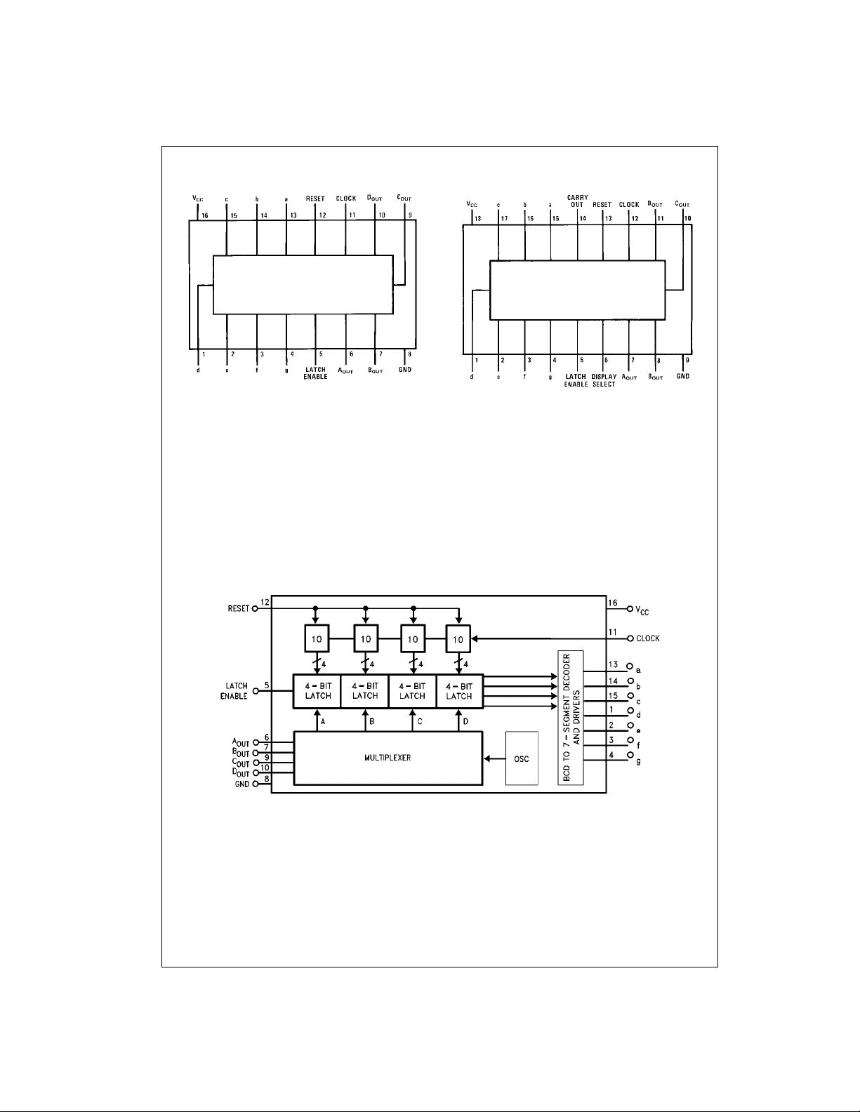
Connection Diagrams
Pin Assignments for DIP
Top View
MM74C925
Functional Description
Reset — Asynchronous, active high
Display Select — High, displays output of counter
Low, displays output of latch
Latch Enable — High, flow through condition
MM74C925 • MM74C926 • MM74C927 • MM74C928
Clock —Negative edge sensitive
Low, latch condition
Logic Diagrams
MM74C926, MM74C927, MM74C928
Segment Output — Current sourcing with 40 mA @V
Digit Output — Current sourcing with 1 mA @V
Carry-Out — 2 LTTL loads. See carry-out waveforms.
MM74C925
V
CC
LTTL loads
1.75V. Also, sink capability = 2 LTTL loads
Top View
− 1.6V (typ.) Also, sink capability = 2
OUT
OUT
=
=
www.fairchildsemi.com 2

Logic Diagrams (Continued)
MM74C925 • MM74C926 • MM74C927 • MM74C928
MM74C926
MM74C927
MM74C928
3 www.fairchildsemi.com
 Loading...