查询MM74C914供应商
MM74C914
Hex Schmitt Trigger with Extended Input Voltage
MM74C914 Hex Schmitt Trigger with Extended Input Voltage
October 1987
Revised January 1999
General Description
The MM74C914 is a monolithic CMOS Hex Schmitt t r igger
with special input protection scheme. This scheme allows
the input voltage levels to exceed V
−25V to GND + 25V), and is valuable for applica-
10V (V
CC
tions involving voltage level shifting or mismatched power
supplies.
The positive and negative-going threshold voltages, V
and VT−, show low variation with respect to temperature
or ground by at least
CC
(typ 0.0005V/°C at V
≥ 0.2 VCC is guaranteed.
V
T−
Features
■ Hysteresis: 0.45 VCC (typ.) 0.2 VCCguaranteed
■ Special input protection: Extended Input Voltage
Range
T+
■ Wide supply voltage range: 3V to 15V
■ High noise immunity: 0.7 V
■ Low power TTL compatibility: Fan out of 2 driving 74L
= 1 0V). And the hysteresis, VT+ −
CC
(typ.)
CC
Ordering Code:
Order Number Package Number Package Description
MM74C914M M14A 14-Lead Small Outline Integrated Circuit (SOIC), JEDEC MS-120, 0.150” Narrow
MM74C914N N14A 14-Lead Plastic Dual-In-Line Package (PDIP), JEDEC MS-001, 0.300” Wide
Device also available in Tape and Reel. Specify by appendin g s uf f ix let t er “X” to the ordering co de.
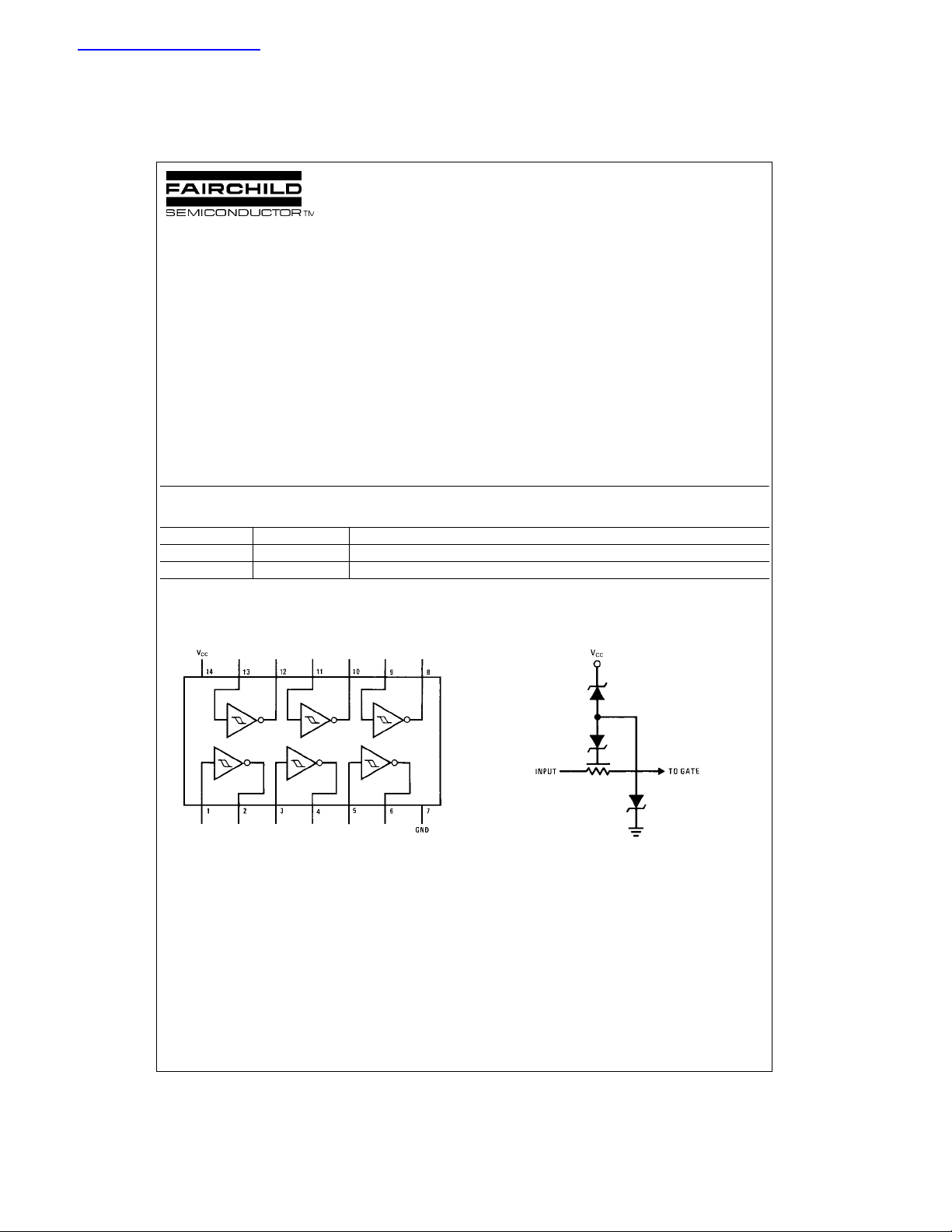
Connection Diagrams
Pin Assignments for DIP
Special Input Protection
Top View
© 1999 Fairchild Semiconductor Corporation DS005917.prf www.fairchildsemi.com
8V ≈ 25V
for the diodes.

Absolute Maximum Ratings(Note 1)
Voltage at any Input Pin VCC − 25V to GND + 25V
Voltage at any other Pin −0.3Vto V
Operating Temperature Range (T
MM74C914
Storage Temperature Range (T
) −40°C to +85°C
A
) −65°C to +150°C
S
Power Dissipation
Dual-In-Line 700 mW
Small Outline 500mW
CC
Operating V
Absolute Maximum (V
Lead Temperature (T
+ 0.3V
(Soldering, 10 seconds) 300°C
Note 1: “Absolute Maxi mum Ratings” are those valu es beyond which the
safety of the device cannot be guaranteed. Ex ce pt for “O perating Temperature Range”, they are not mean t to imply that the device s should be operated at these limits. The Electrical Charac t eristics tables provide co nditions
for actual device operation.
Range 3V to 15V
CC
) 18V
CC
)
L
DC Electrical Characteristics
Min/Max limits apply across temperature range unless otherwise noted
Symbol Parameter Conditions Min Typ Max Units
CMOS TO CMOS
V
T+
V
T−
VT+ − V
V
OUT(1)
V
OUT(0)
I
IN(1)
I
IN(0)
I
CC
CMOS/LPTTL INTERFACE
V
IN(1)
V
IN(0)
V
OUT(1)
V
OUT(0)
OUTPUT DRIVE (See Family Characteristics Data Sheet) (Short Circuit Current)
I
SOURCE
I
SOURCE
I
SINK
I
SINK
Note 2: Only one input is at ½ VCC, the others are either at VCC or GND.
Positive Going Threshold Voltage VCC = 5V 3.0 3.6 4.3 V
Negative Going Threshold Voltage VCC = 5V 0.7 1.4 2.0 V
Hysteresis VCC = 5V 1.0 2.2 3.6 V
T−
Logical“1” Output Voltage VCC = 5V, IO = −10 µA4.5 V
Logical “0” Output Voltage VCC = 5V, IO = +10 µA0.5V
Logical “1” Input Current VCC = 15V, VIN = 25V 0.005 5.0 µA
Logical “0” Input Current VCC = 15V, VIN = −10V −100 −0.005 µA
Supply Current VCC = 15V, VIN = − 10V/25V 0.05 300 µA
Logical “1” Input Voltage VCC = 5V 4.3 V
Logical “0” Input Voltage VCC = 5V 0.7 V
Logical “1” Output Voltage VCC = 4.75V, IO = −360 µA2.4 V
Logical “0” Output Voltage VCC = 4.75V, IO = 360 µA0.4V
Output Source Current VCC = 5V, V
(P-Channel)
Output Source Current VCC = 10V, V
(P-Channel)
Output Sink Current VCC = 5V, V
(N-Channel)
Output Sink Current VCC = 10V, V
(N-Channel)
VCC = 10V 6.0 6.8 8.6 V
VCC = 15V 9.0 10 12.9
VCC = 10V 1.4 3.2 4.0 V
VCC = 15V 2.1 5 6.0
VCC = 10V 2.0 3.6 7.2 V
VCC = 15V 3.0 5 10.8 V
VCC = 10V, IO = −10 µA9.0 V
VCC = 10V, IO = +10 µA1.0V
VCC = 5V, VIN = − 2.5V (Note 2) 20 µA
VCC = 10V, VIN = 5V (Note 2) 200 µA
VCC = 15V, VIN = 7.5V (Note 2) 600 µA
= 0V, TA = 25°C −1.75 −3.3 mA
OUT
= 0V, TA = 25°C −8.0 −15 mA
OUT
= VCC, TA = 25°C 1.75 3.6 mA
OUT
= VCC, TA = 25°C8.016 mA
OUT
www.fairchildsemi.com 2
 Loading...