查询MM74C912供应商
MM74C912
6-Digit BCD Display Controller/Driver
MM74C912 6-Digit BCD Display Controller/Driver
October 1987
Revised January 1999
General Description
The MM74C912 display contr oller s are interface el emen ts,
with memory, that drive a 6-digit, 8-segment LED display.
The display controllers receive data infor mation through 5
data input s A, B, C, D an d DP, and digit i n f o rmat i o n th ro ug h
3 address inputs K1, K2 and K3.
The input data is wr itten into the register se lected by the
address information when CHIP ENABLE, (CE
WRITE ENABLE, (WE
either CE
required. A self-contained internal oscillator sequentially
presents the stored da ta to a decoder where 4 data bits
control the format of the displayed character an d 1 bit co ntrols the decimal point. The internal oscillator is controlled
by a control input labeled OSCILLATOR ENABLE, (OSE
which is tied LOW in normal operation. A high level at OSE
prevents automatic refresh of the display.
The 7-segment plus decimal point output information
directly drives an LE D display through high dr ive (100 mA
or WE return HIGH. Data hold time is not
), are LOW and is latched when
), and
typ.) output drivers. The drivers are active when the control
pin labeled SEGMENT OUTPUT ENABLE, (SOE
and go into 3-STATE when SOE
allows for duty cycle bright ness control and for disabling
the output drivers for power conservati on.
The MM74C912 segment de coder conver ts BCD data into
7-segment format.
All inputs are TTL compati ble and do not clam p to the V
supply.
is HIGH. This feature
Features
■ Direct segment drive (100 mA typ.) 3-STATE
■ 6 registers addressed like RAM
■ Internal oscillator and scanning circuit
),
■ Direct base drive to digit transistor (20 mA typ.)
■ Internal segment decoder
■ TTL compatible inputs
Ordering Code:
Order Number Package Number Package Description
MM74C912N N28B 28-Lead Plastic Dual-In-Line Package (PDIP), JEDEC MS-010, 0.600” Wide
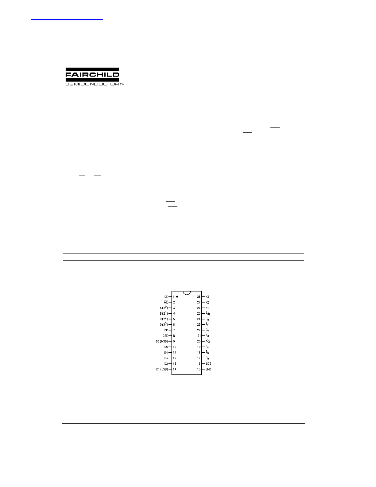
Connection Diagram
Dual-In-Line Package
), is LOW
CC
Top View
© 1999 Fairchild Semiconductor Corporation DS005916.prf www.fairchildsemi.com

Truth Tables
MM74C912
X = Don’t Care
Input Contr o l
CE Digit Address WE Operation
K3 K2 K1
00000Write Digit 1
00001Latch Digit 1
00010Write Digit 2
00011Latch Digit 2
00100Write Digit 3
00101Latch Digit 3
00110Write Digit 4
00111Latch Digit 4
01000Write Digit 5
01001Latch Digit 5
01010Write Digit 6
01011Latch Digit 6
01100Write Null Digit
01101Latch Null Digit
01110Write Null Digit
01111Latch Null Digit
1XXXXDisable Writing
Output Control
SOE
0 0 Refresh Display
0 1 Stop Oscillator (Note 1)
1 0 Disable Segment Outputs
1 1 Standby Mode
Note 1: Segment drive may exceed maximum display dissip at ion.
www.fairchildsemi.com 2
OSE Operation

Functional Description
MM74C912
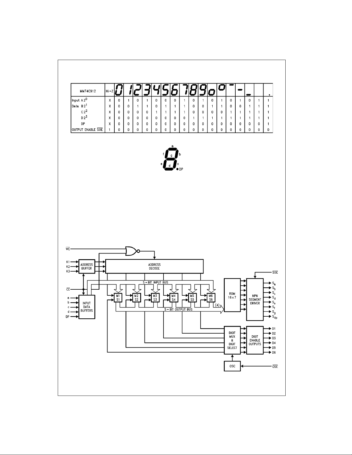
Character Font
Segment Identi fic at i on
The MM74C912 display controll er is manufactured using
metal gate CMOS technology. A single 5V 74 series TTL
supply can be used for power and shou ld be bypassed at
pin.
the V
CC
All inputs are TTL co mpatible; the segment outputs dr ive
the LED display directly through current limiting resistors.
The digit outputs ar e desi gned to dir ectly dr ive the base of
Block Diagram
a grounded emitte r digit transistor without the ne ed of a
Darlington configuration.
As seen in the block diagram, these display controllers
contain six 5-bit register s; any one of which may be randomly written. Th e internal multi plexer scans the registers
and refreshes the di splay. This combination of write only
memory and self-scan display makes the display controller
a “refreshing experi ence” for an over-burdened microprocessor.
3 www.fairchildsemi.com
 Loading...