Fairchild MM74C905 service manual

查询MM74C905供应商
MM74C905
12-Bit Successive Approximation Register
MM74C905 12-Bit Successive Appro ximation Register
October 1987
Revised January 1999
General Description
The MM74C905 CMOS 12-bit successive approximation
register contains all the digit control and storage necessary
for successive approximation analog-to-digita l conversion.
Because of the unique capability of CMOS to switch to
each supply rail without any offset voltage, it can also be
used in digital systems as the con trol and st orag e element
in repetitive routines.
Features
■ Wide supply voltage range: 3.0V to 15V
■ Guaranteed noise margin: 1.0V
■ High noise immunity: 0.45 V
■ Low power TTL compatibility: Fan out of 2 driving 74L
■ Provision for register extension or truncation
■ Operates in START/STOP or continuous conversion
mode
■ Drive ladder switches directly. For 10 bits or less with
50k/100k R/2R ladder network
CC
(typ)
Ordering Code:
Order Number Package Number Package Description
MM74C905N N24A 24-Lead Plastic Dual-In-Line Package (PDIP), JEDEC MS-010, 0.600” Wide
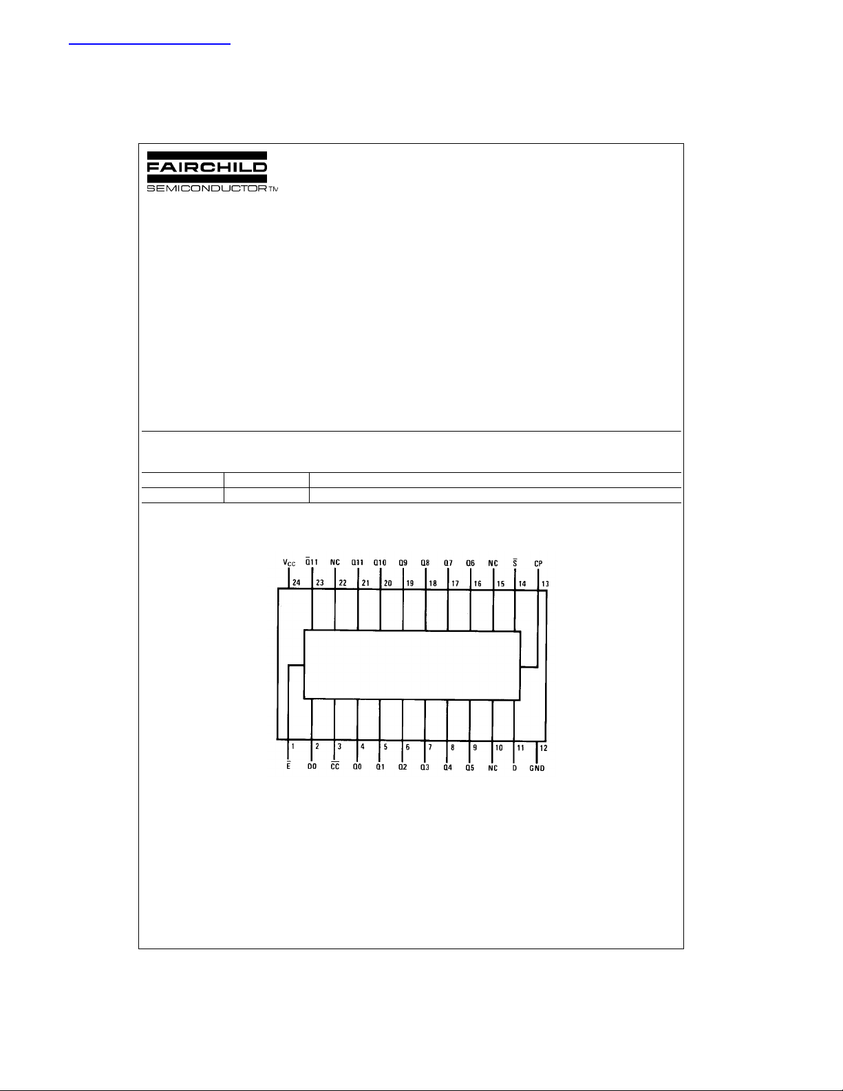
Connection Diagram
Pin Assignments for DIP
© 1999 Fairchild Semiconductor Corporation DS005910.prf www.fairchildsemi.com

Truth Table
Time Inputs Outputs
MM74C905
t
n
DSE D0 Q11 Q10 Q9 Q8 Q7 Q6 Q5 Q4 Q3 Q2 Q1 Q0 CC
0 XLLX X X XXXXXXXXXXX
1D11HLX L H HHHHHHHHHHH
2D10HLD11D11L HHHHHHHHHHH
3D9HLD10D11D10LHHHHHHHHHH
4D8HLD9D11D10D9LHHHHHHHHH
5D7HLD8D11D10D9D8LHHHHHHHH
6D6HLD7D11D10D9D8D7LHHHHHHH
7D5HLD6D11D10D9D8D7D6LHHHHHH
8D4HLD5D11D10D9D8D7D6D5LHHHHH
9D3HLD4D11D10D9D8D7D6D5D4LHHHH
10 D2 H L D3 D11 D10 D9 D8 D7 D6 D5 D4 D3 L H H H
11 D1 H L D2 D11 D10 D9 D8 D7 D6 D5 D4 D3 D2 L H H
12 D0 H L D1 D11 D10 D9 D8 D7 D6 D5 D4 D3 D2 D1 L H
13 X H L D0D11D10D9D8D7D6D5D4D3D2D1D0 L
14 X X L X D11 D10 D9 D8 D7 D6 D5 D4 D3 D2 D1 D0 L
X X H X H NC NCNCNCNCNCNCNCNCNCNCNC
H = HIGH Level
L = LOW Level
X = Don’t Care
NC = No Change
www.fairchildsemi.com 2

Absolute Maximum Ratings(Note 1)
Voltage at Any Pin −0.3V to VCC+0.3V
Operating Temperature Range (T
Storage Temperature Range (T
Power Dissipation (P
)
D
Dual-In-Line 700 mW
Small Outline 500 mW
Operating V
Range 3.0V to 15V
CC
) −40°C to +85°C
A
) −65°C to +150°C
S
Absolute Maximum V
Lead Temperature (T
CC
)
L
(Soldering, 10 seconds) 260°C
Note 1: “Absolute Maximum Rat ings” are tho se values beyond which the
safety of the device cannot be guaranteed. E x c ept for “ Operating Temperature Range” they are not mea nt to imply that the devices sh ould be operated at these limits. The table of “Electrical Characteristics” provides
conditions for actual device o peration.
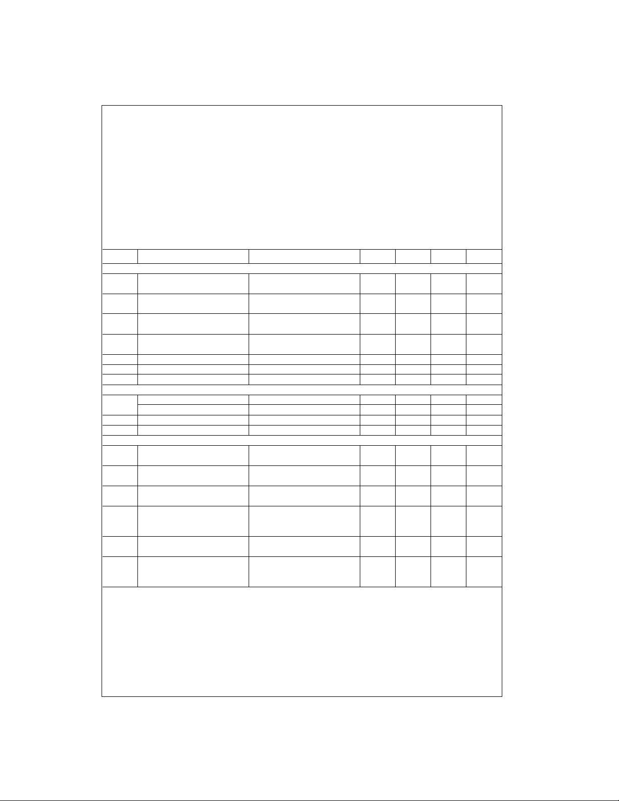
DC Electrical Characteristics
Min/Max limits apply across temperature range unless otherwise noted
Symbol Parameter Conditions Min Typ Max Units
CMOS TO CMOS
V
IN(1)
V
IN(0)
V
OUT(1)
V
OUT(0)
I
IN(1)
I
IN(0)
I
CC
CMOS/LPTTL INTERFACE
V
IN(1)
V
IN(0)
V
OUT(1)
V
OUT(0)
OUTPUT DRIVE (See Family Characteristics Data Sheet)
I
SOURCE
I
SOURCE
I
SINK
I
SINK
R
SOURCE
R
SINK
Logical “1” Input Voltage VCC = 5.0V 3.5 V
VCC = 10V 8.0 V
Logical “0” Input Voltage VCC = 5.0V 1.5 V
VCC = 10V 2.0 V
Logical “1” Output Voltage VCC = 5.0V, IO = −10 µA4.5 V
VCC = 10V, IO = −10 µA9.0 V
Logical “0” Output Voltage VCC = 5.0V, IO = 10 µA0.5V
VCC = 10V, IO = 10 µA1.0V
Logical “1” Input Current VCC = 15V, VIN = 15V 0.005 1.0 µA
Logical “0” Input Current VCC = 15V, VIN = 0V −1.0 −0.005 µA
Supply Current VCC = 15V 0.05 300 µA
Logical “1” Input Voltage VCC = 4.75V VCC − 1.5 V
Logical “0” Input Voltage VCC = 4.75V 0.8 V
Logical “1” Output Voltage VCC = 4.75V, IO = −360 µA2.4 V
Logical “0” Output Voltage VCC = 4.75V, IO = 360 µA0.4V
Output Source Current VCC = 5.0V, V
= 0V −1.75 −3.3 mA
OUT
(P-Channel) TA = 25°C
Output Source Current VCC = 10V, V
= 0V −8.0 −15 mA
OUT
(P-Channel) TA = 25°C
Output Sink Current VCC = 5.0V, V
OUT
= V
CC
1.75 3.6 mA
(N-Channel) TA = 25°C
Output Sink Current VCC = 10V, V
OUT
= V
CC
(N-Channel) TA = 25°C8.016mA
VCC = 10V ±5%
Q11–Q0 Outputs V
= VCC − 0.3V 150 350 Ω
OUT
TA = 25°C
Q11–Q0 Outputs VCC = 10V ±5%
V
= 0.3V 80 230 Ω
OUT
TA = 25°C
MM74C905
16V
3 www.fairchildsemi.com
 Loading...