

查询MM74C193M供应商
MM74C192 • MM74C193
Synchronous 4-Bit Up/Down Decade Counter •
Synchronous 4-Bit Up/Down Binary Counter
January 1991
Revised October 1999
Counter
MM74C192 • MM74C193 Synchronous 4-Bit Up/Down Decade Counter • Synchronous 4-Bit Up/Down Binary
General Description
The MM74C192 and MM74C193 up/down counters are
monolithic complementary MOS (CMOS) integrated circuits. The MM74C192 is a BCD counter, while the
MM74C193 is a binary counter.
Counting up and counting do wn is pe rform ed by tw o count
inputs, one being hel d hig h whil e the other is cloc ked. T he
outputs change on the positive-going transition of this
clock.
These counters feature preset inputs that are set when
load is a logical “0” and a clear which forces all o utputs to
“0” when it is at a logical “1”. The counter s also have car ry
and borrow outputs so th at t hey can be cascaded using no
external circuitry.
Features
■ High noise margin: 1V guaranteed
■ Tenth power TTL compatible: Drive 2 LPTTL loads
■ Wide supply range: 3V to 15V
■ Carry and borrow outputs for N-bit cascading
■ Asynchronous clear
■ High noise immunity: 0.45 V
CC
(typ.)
Ordering Code:
Order Number Package Number Package Description
MM74C192N N16E 16-Lead Plastic Dual-In-Line Package (PDIP), JEDEC MS-001, 0.300” Wide
MM74C193M M16A 16-Lead Small Outline Integrated Circuit (SOIC), JEDEC MS-012, 0.150” Narrow
MM74C193N N16E 16-Lead Plastic Dual-In-Line Package (PDIP), JEDEC MS-001, 0.300” Wide
Device also available in Tape and Reel. Specify by appending s uffix let te r “X” to the ordering code .
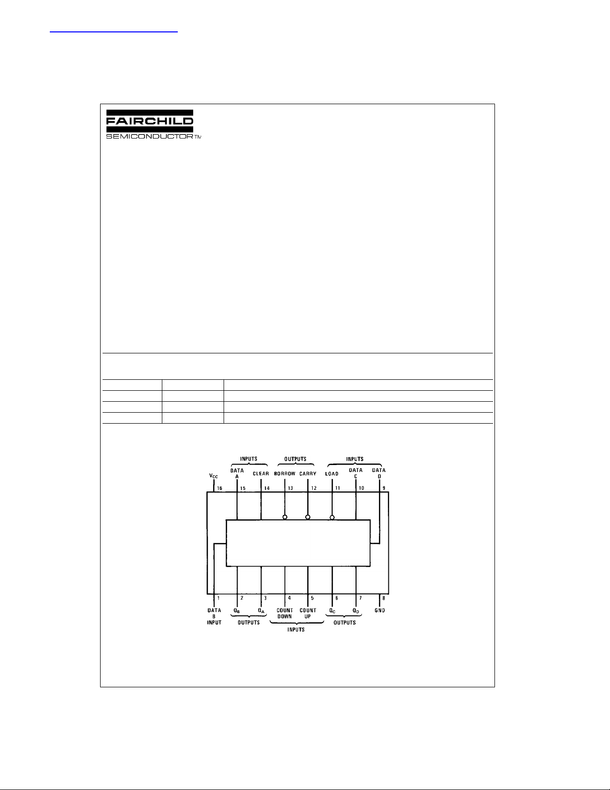
Connection Diagram
Top View
© 1999 Fairchild Semiconductor Corporation DS005901 www.fairchildsemi.com
Absolute Maximum Ratings(Note 1)
Voltage at Any Pin −0.3V to VCC + 0.3V
Operating Temperature Range (T
Storage Temperature Range (T
Maximum V
Power Dissipation (P
Voltage 18V
CC
)
D
Dual-In-Line 700 mW
Small Outline 500 mW
Operating V
Lead Temperature (T
MM74C192 • MM74C193
(Soldering, 10 seconds) 260°C
Range 3V to 15V
CC
)
A
) −40°C to +85°C
A
) −65°C to +150°C
S
Note 1: “Absolute Maximum Ratings” ar e those value s beyond which the
safety of the device cannot be guaranteed. Except for “Operating Temperature Range” they are not m eant to i mply that t he devices should be operated at these limits. The Electrical Charac te ris t ic s ta ble provides conditions
for actual device operation.
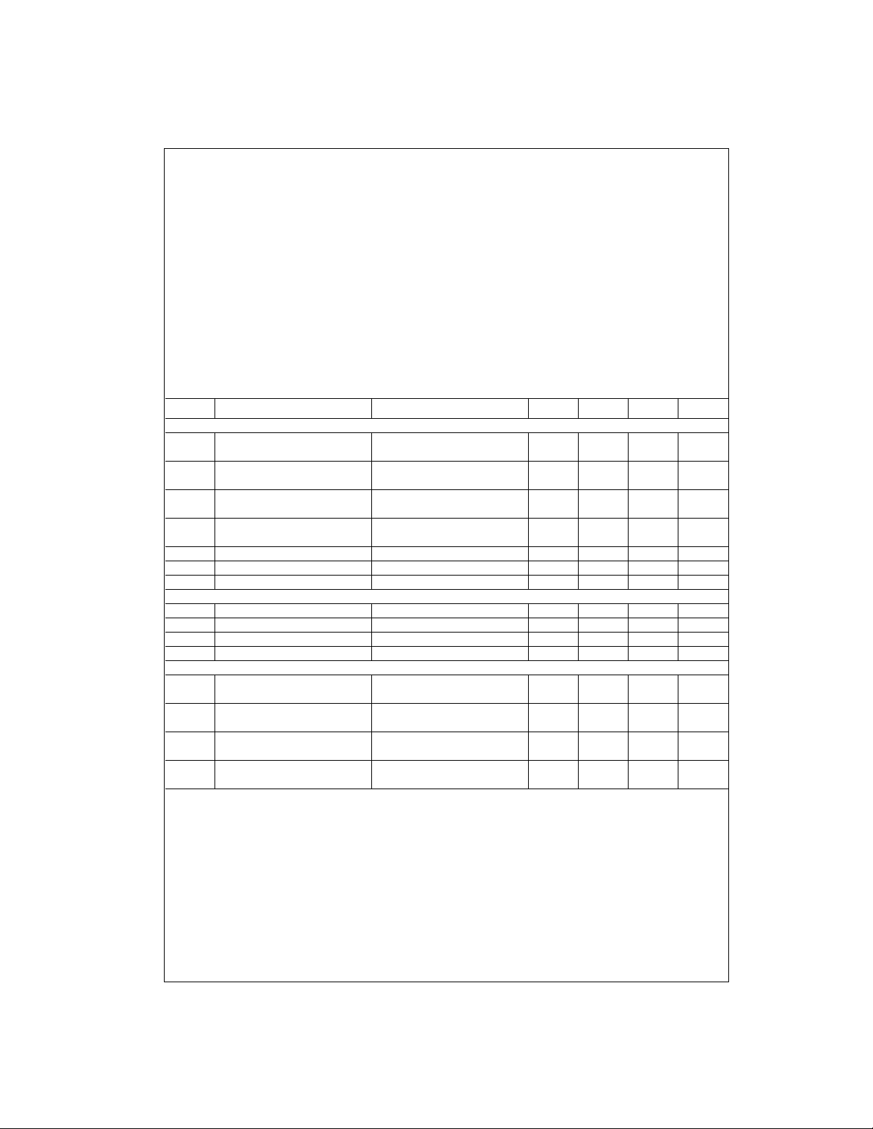
DC Electrical Characteristics
Min/Max limits apply across temperature range unless otherwise noted
Symbol Parameter Conditions Min Typ Max Units
CMOS TO CMOS
V
IN(1)
V
IN(0)
V
OUT(1)
V
OUT(0)
I
IN(1)
I
IN(0)
I
CC
CMOS TO LPTTL INTERFACE
V
IN(1)
V
IN(0)
V
OUT(1)
V
OUT(0)
OUTPUT DRIVE (See Family Characteristics Data Sheet) (Short Circuit Current)
I
SOURCE
I
SOURCE
I
SINK
I
SINK
Logical “1” Input Voltage VCC = 5V 3.5 V
V
= 10V 8.0 V
CC
Logical “0” Input Voltage VCC = 5V 1.5 V
VCC = 10V 2.0 V
Logical “1” Output Voltage VCC = 5V, IO = −10 µA4.5 V
VCC = 10V, IO = −10 µA9.0 V
Logical “0” Output Voltage VCC = 5V, IO = 10 µA0.5V
VCC = 10V, IO = 10 µA1.0V
Logical “1” Input Current VCC = 15V, VIN = 15V 0.005 1.0 µA
Logical “0” Input Current VCC = 15V, VIN = 0V −1.0 −0.005 µA
Supply Current VCC = 15V 0.05 300 µA
Logical “1” Input Voltage VCC = 4.75V VCC − 1.5 V
Logical “0” Input Voltage VCC = 4.75V 0.8 V
Logical “1” Output Voltage VCC = 4.75V, IO = −100 µA2.4 V
Logical “0” Output Voltage VCC = 4.75V, IO = 360 µA0.4V
Output Source Current VCC = 5V, V
TA = 25°C, V
Output Source Current VCC = 10V, V
TA = 25°C, V
Output Sink Current VCC = 5V, V
TA = 25°C, V
Output Sink Current VCC = 10V, V
TA = 25°C, V
= 0V −1.75 mA
IN(0)
= 0V
OUT
= 0V −8mA
IN(0)
= 0V
OUT
= 5V 1.75 mA
IN(1)
= V
OUT
CC
= 10V 8 mA
IN(1)
= V
OUT
CC
www.fairchildsemi.com 2

AC Electrical Characteristics (Note 2)
= 25°C, CL = 50 pF, unless otherwise noted
T
A
Symbol Parameter Conditions Min Typ Max Units
t
pd
t
pd
t
pd
t
S
t
W
t
W
t
pd0
t
pd1
t
W
f
MAX
t
r
t
f
C
IN
C
PD
Note 2: AC Parameters are guaranteed by DC c orrelated testing.
Note 3: Capacitance is guaranteed by periodic t es t ing.
Note 4: C
Propagation Delay VCC = 5V 250 400 ns
Time to Q from Count Up or Down VCC = 10V 100 160 ns
Propagation Delay VCC = 5V 120 200 ns
Time to Q Borrow from Count Down VCC = 10V 50 80 ns
Propagation Delay VCC = 5V 120 200 ns
Time to Carry from Count Up VCC = 10V 50 80 ns
Time Prior to Load VCC = 5V 100 160 ns
that Data Must be Present V
= 10V 30 50 ns
CC
Minimum Clear Pulse Width VCC = 5V 300 480 ns
= 10V 120 190 ns
V
CC
Minimum Load Pulse Width VCC = 5V 100 160 ns
= 10V 40 65 ns
V
CC
Propagation Delay VCC = 5V 300 480 ns
Time to Q from Load VCC = 10V 120 190 ns
Minimum Count Pulse Width VCC = 5V 120 200 ns
VCC = 10V 35 80 ns
Maximum Count Frequency VCC = 5V 2.5 4 MHz
= 10V 6 10 MHz
V
CC
Count Rise and Fall Time VCC = 5V 15 µs
VCC = 10V 5 µs
Input Capacitance (Note 3) 5 pF
Power Dissipation Capacitance (Note 4) 100 pF
determines the no load AC power consump t ion of any CMOS device. F or c omplete explanation, see Application Note AN -90.
PD
MM74C192 • MM74C193
Cascading Packages
Guaranteed Noise Margin
as a Function of V
CC
3 www.fairchildsemi.com

Timing Diagrams
MM74C192 • MM74C193
Note A: Clear outputs to zero.
Note B: Load (preset) to binary thirteen.
Note C: Count up to fourteen, fifteen, carry, zero, one and two.
Note D: Count down to one, zero, borrow, fifteen, fourteen, and thirteen.
MM74C192
MM74C193
Note A: Clear outputs to zero.
Note B: Load (preset) to BCD seven.
Note C: Count up to eight, nine, carry, zero, one, and two.
Note D: Count down to one, zero, borrow, nine, eight, and seven.
Note E: Clear overrides load, data, and count inputs.
Note F: When counting up, count down input must be HIGH; when counting down, count-up input must be HIGH.
www.fairchildsemi.com 4

Physical Dimensions inches (millimeters) unless otherwise noted
MM74C192 • MM74C193
16-Lead Small Outline Integrated Circuit (SOIC), JEDEC MS-012, 0.150” Narrow
Package Number M16A
5 www.fairchildsemi.com

Physical Dimensions inches (millimeters) unless otherwise noted (Continued)
Counter
16-Lead Plastic Dual-In-Line Package (PDIP), JEDEC MS-001, 0.300” Wide
Fairchild does not assume any responsibility for us e of any circuitry described, no circuit patent licenses are implied and
Fairchild reserves the right at any time without notice to change said circuitry and specifications.
LIFE SUPPORT POLICY
FAIRCHILD’S PRODUCTS ARE NOT AUTHORIZED FOR USE AS CRITICAL COMPONENTS IN LIFE SUPPORT
DEVICES OR SYSTEMS WITHOUT THE EXPRESS WRITTEN APPROVAL OF THE PRESIDENT OF FAIRCHILD
SEMICONDUCTOR CORPORATION. As used herein:
1. Life support devices or systems are devices or syste ms
which, (a) are intended for surgical implant into the
body, or (b) support or sustain life, and (c) whose failure
MM74C192 • MM74C193 Synchronous 4-Bit Up/Down Decade Counter • Synchronous 4-Bit Up/Down Binary
to perform when properly used in accordance with
instructions for use provided in the labeling, can be reasonably expected to result in a significan t injury to the
user.
Package Number N16E
2. A critical component in any compon ent of a lif e supp ort
device or system whose failu re to perform can be reasonably expected to ca use the fa i lure of the li fe su pp ort
device or system, or to affect its safety or effectiveness.
www.fairchildsemi.com
www.fairchildsemi.com 6
 Loading...