

Fairchild MM74C175 service manual
查询MM74C175供应商
MM74C175
Quad D-Type Flip-Flop
MM74C175 Quad D-Type Flip-Flop
October 1987
Revised January 1999
General Description
The MM74C175 consis ts of four positive-edge triggered D type flip-flops implemented with monolithic CMOS technology. Both are true and compleme nted outputs from each
flip-flop are externally available. All four flip-flops are controlled by a common clock and a common clear. Information at the D-type inputs meeting the set-up time
requirements is transferred t o the Q outputs on the positive-going edge of the clock pulse. The clear ing operation,
enabled by a negative pulse at Clear input, clears all four Q
outputs to logical “0” and Q's to logical “1”.
All inputs are protected from static discharge by diode
clamps to V
and GND.
CC
Features
■ Wide supply voltage range: 3V to 15V
■ Guaranteed noise margin: 1.0V
■ High noise immunity: 0.45 V
■ Low power TTL compatibility: Fan out of 2 driving 74L
CC
(typ.)
Ordering Code:
Order Number Package Number Package Description
MM74C175M M16A 16-Lead Small Outline Integrated Circuit (SOIC), JEDEC MS-012, 0.150” Narrow
MM74C175N N16E 16-Lead Plastic Dual-In-Line Package (PDIP), JEDEC MS-001, 0.300” Wide
Device also available in Tape and Reel. Specify by appendin g s uf f ix let t er “X” to the ordering code.
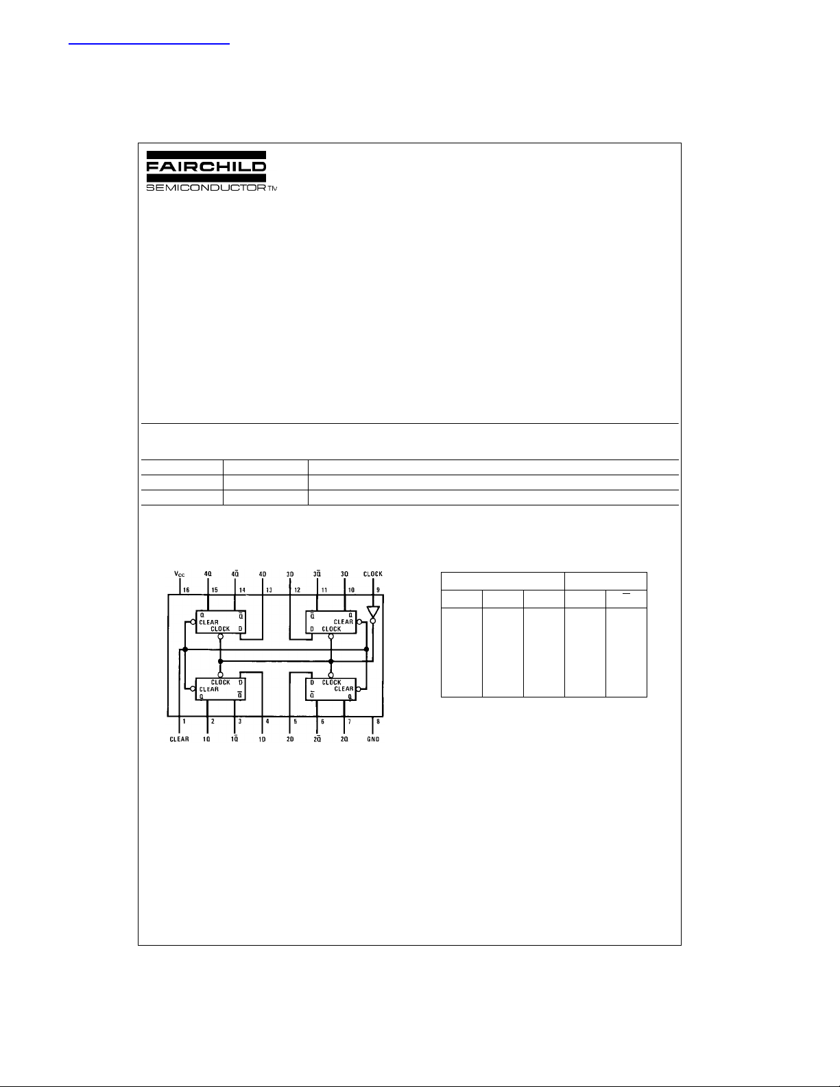
Connection Diagram
Pin Assignments for DIP and SOIC
Top View
Truth Table
Each Flip-Flop
Inputs Outputs
Clear Clock D Q Q
LXXLH
H ↑ HHL
H ↑ LLH
HHXNCNC
HLXNCNC
H = HIGH Level
L = LOW Level
X = Irrelevant
↑ = Transition from LOW-to-HIGH level
NC = No Change
© 1999 Fairchild Semiconductor Corporation DS005900.prf www.fairchildsemi.com
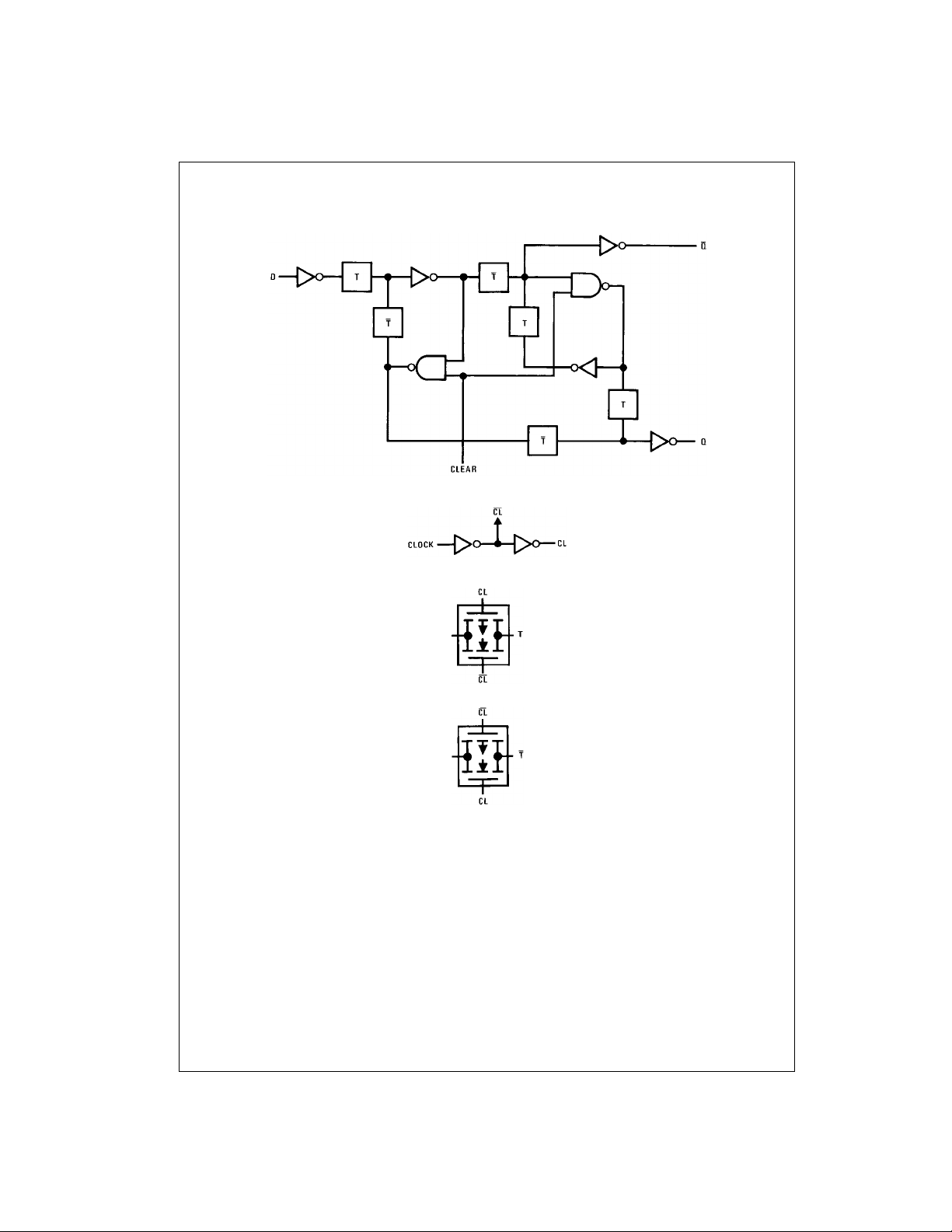
Block Diagrams
MM74C175
Typical One of Four
www.fairchildsemi.com 2
 Loading...