Fairchild MM74C165 service manual

查询MM74165N供应商
MM74C165
Parallel-Load 8-Bit Shift Register
MM74C165 Parallel-Load 8-Bit Shift Register
October 1987
Revised January 1999
General Description
The MM74C165 func tions as an 8-bit parallel- load, serial
shift register. Data is loaded into the register i ndependent
of the state of the clock(s) when PARALLEL LOAD (PL
low. Shifting is inhibited as long as PL
sequentially shifted from com plementary outputs, Q
, highest-order bit (P7) first. New serial data may be
Q
7
entered via the SERIAL DATA (Ds) input. Serial shifting
occurs on the r ising edge of CL OCK1 or CLOCK2. C lock
inputs may be used separately o r together for combined
clocking from independent sou rces. Either clock input m ay
be used also as an active-low clock enable. To prevent
double-clocking when a clock input is used as an e nable,
is low. Data is
7
the enable must be changed to a hi gh level (disabled) on ly
while the clock is HIGH.
Features
) is
■ Wide supply voltage range: 3V to 15V
and
■ Guaranteed noise margin: 1V
■ High noise immunity: 0.45 V
■ Low power TTL compatibility: fan out of 2 driving 74L
■ Parallel loading independent of clock
■ Dual clock inputs
■ Fully static operation
CC
(typ.)
Ordering Code:
Order Number Package Number Package Description
MM74165N N16E 16-Lead Plastic Dual-In-Line Package (PDIP), JEDEC MS-001, 0.300” Wide
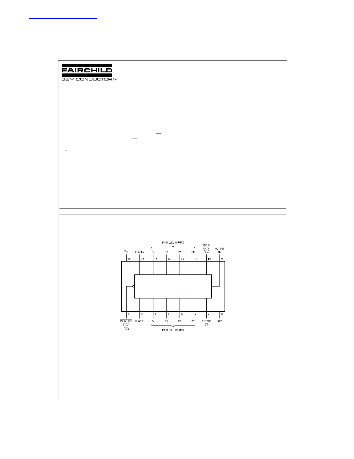
Connection Diagram
Pin Assignments for DIP
Top View
© 1999 Fairchild Semiconductor Corporation DS005897.prf www.fairchildsemi.com

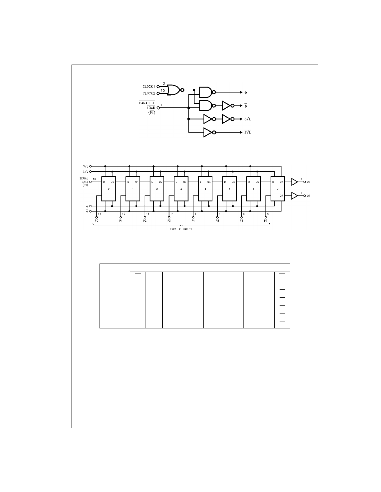
Block Diagrams
MM74C165
*Please look into S ec t ion 8, Appendix D for availability of vari ous package types.
Truth Table
State Inputs Internal Outputs
Clock1 Clock2 Ds P0 thru P7 Q0 Q1 Q7 Q7
PL
(as enable)
Parallel Load L X X X P0…P7P0P1P7P7
Enable H L L X X P0P1P7P7
Shift (with Ds) H ↑ L H X H P0 P6 P6
Shift (with Ds) H ↑ LLXLHP5P5
Hold (Disable) H ↑ HXXLHP5P5
X = Don’t Care
H = V
IN(1)
L = V
IN(0)
↑ = Clock transition from V
P0 thru P7 = Data present (and loaded into) parallel inputs
Q0 thru Q6 = Internal flip-flop outputs
www.fairchildsemi.com 2
IN(0)
to V
IN(1)
 Loading...