查询MM74C08N供应商
MM74C08
Quad 2-Input AND Gate
MM74C08 Quad 2-Input AND Gate
October 1987
Revised January 2004
General Description
The MM74C08 employs complementary MOS (CMOS)
transistors to achieve wide powe r supply operating range,
low power consumption and high noise margin, these
gates provide basic functions used in the implementation of
digital integrated circuit systems. The N- and P-channel
enhancement mode transistors provid e a symmetrical c ircuit with output swing essentially equal to the supply voltage. No DC power other than that caused by leakage
current is consumed during static condition. All inputs are
protected from dama ge due to static discharge by diode
clamps to V
and GND.
CC
Features
■ Wide supply voltage range: 3.0V to 15V
■ Guaranteed noise margin: 1.0V
■ High noise immunity: 0.45 V
■ Low power TTL compatibility:
Fan out of 2 driving 74L
■ Low power consumption: 10 nW/package (typ.)
CC
(typ.)
Ordering Code:
Order Number Package Number Package Description
MM74CD8N N14A 14-Lead Plastic Dual-In-Line Package (PDIP), JEDEC MS-001, 0.300" Wide
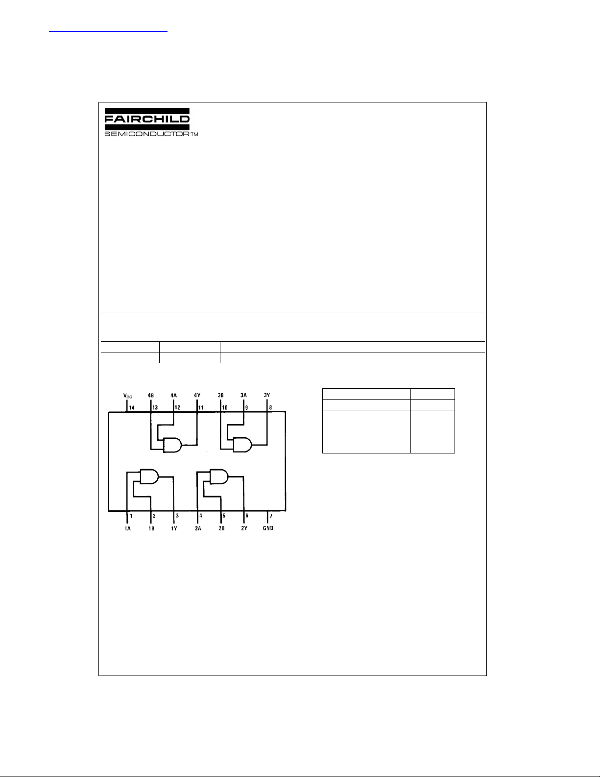
Connection Diagram
Truth Table
ABY
LLL
LHL
HLL
HHH
H = HIGH Level
L = LOW Level
Inputs Outputs
Top View
© 2004 Fairchild Semiconductor Corporation DS005878 www.fairchildsemi.com

Absolute Maximum Ratings(Note 1)
Voltage at Any Pin −0.3V to VCC + 0.3V
Operating Temperature Range
MM74C08
Storage Temperature Range
Power Dissipation (P
)
D
−55°C to +125°C
−65°C to +150°C
Dual-In-Line 700 mW
Small Outline 500 mW
Operating V
Absolute Maximum V
Range 3.0V to 15V
CC
CC
Lead Temperature
(Soldering, 10 seconds) 260
Note 1: “Absolute Maximum Ratings” are those values beyond which the
safety of th e device cannot be guaranteed. Ex cept for “Operating Temperature Range” they are not m eant to i mply that the devic es should be oper-
18V
ated at these limits. The Electrical Chara c te ris t ic s ta ble provides condit ions
for actual device operation.
°C
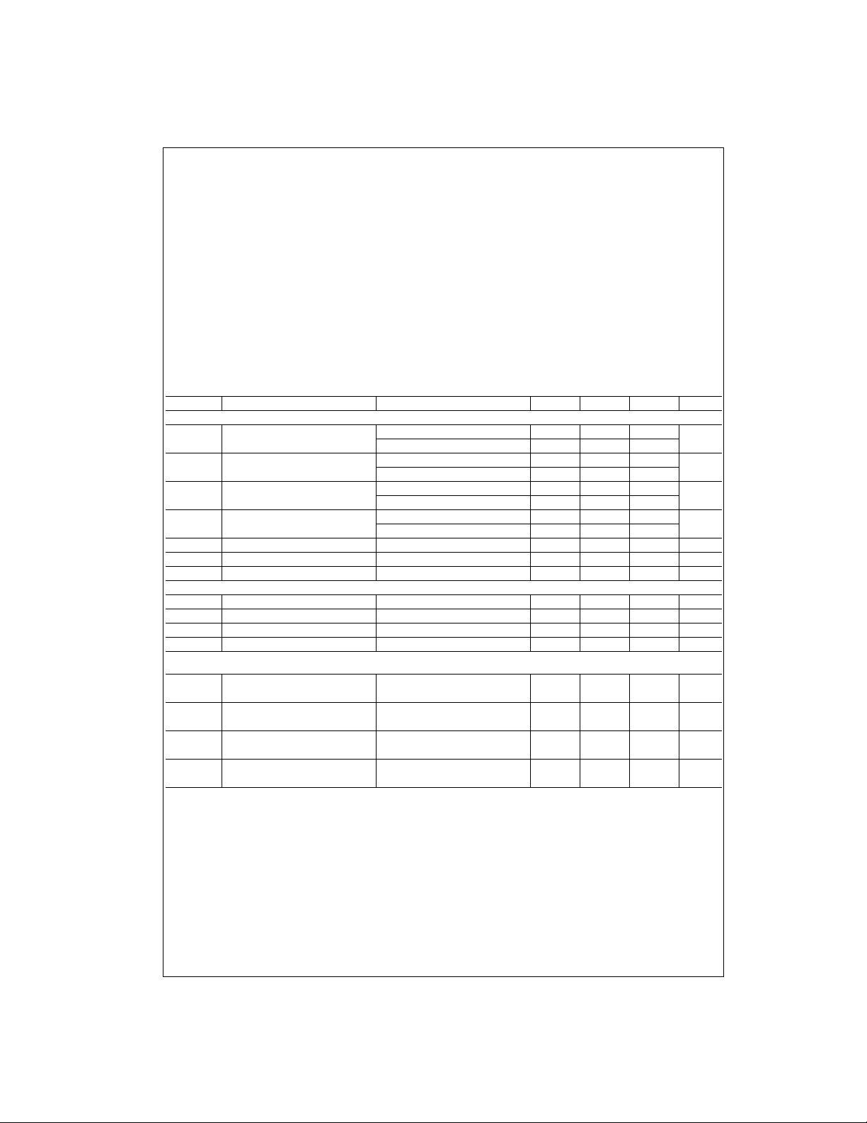
DC Electrical Characteristics
Min/Max limits apply across the guaranteed temperature range, unless otherwise noted
Symbol Parameter Conditions Min Typ Max Units
CMOS TO CMOS
V
IN(1)
V
IN(0)
V
OUT(1)
V
OUT(0)
I
IN(1)
I
IN(0)
I
CC
CMOS/LPTTL INTERFACE
V
IN(1)
V
IN(0)
V
OUT(1)
V
OUT(0)
OUTPUT DRIVE (see Family Characteristics Data Sheet) TA = 25°C (short circuit current)
I
SOURCE
I
SOURCE
I
SINK
I
SINK
Logical “1” Input Voltage VCC = 5.0V 3.5
VCC = 10V 8.0
Logical “0” Input Voltage VCC = 5.0V 1.5
V
= 10V 2.0
CC
Logical “1” Output Voltage VCC = 5.0V, IO = −10 µA4.5
VCC = 10V, IO = −10 µA9.0
Logical “0” Output Voltage VCC = 5.0V, IO = 10 µA0.5
= 10V, IO = 10 µA1.0
V
CC
Logical “1” Input Current VCC = 15V, VIN = 15V 0.005 1.0 µA
Logical “0” Input Current VCC = 15V, VIN = 0V −1.0 −0.005 µA
Supply Current VCC = 15V 0.01 15 µA
Logical “1” Input Voltage 74C, VCC = 4.75V VCC − 1.5 V
Logical “0” Input Voltage 74C, VCC = 4.75V 0.8 V
Logical “1” Output Voltage 74C, VCC = 4.75V, IO = −360 µA2.4 V
Logical “0” Output Voltage 74C, VCC = 4.75V, IO = 360 µA0.4V
Output Source Current VCC = 5.0V, V
= 0V −1.75 −3.3 mA
OUT
(P-Channel)
Output Source Current VCC = 10V, V
= 0V −8.0 15 mA
OUT
(P-Channel)
Output Sink Current VCC = 5.0V, V
OUT
= V
CC
1.75 3.6 mA
(N-Channel)
Output Sink Current VCC = 10V, V
OUT
= V
CC
8.0 16 mA
(N-Channel)
V
V
V
V
www.fairchildsemi.com 2
 Loading...