现货库存、技术资料、百科信息、热点资讯,精彩尽在鼎好!
LM555/NE555/SA555
Single Timer
Features
Features
FeaturesFeatures
• High Current Drive Capability (200mA)
• Adjustable Duty Cycle
• Tem perature Stability of 0.005%/°C
• Timing From µSec to Hours
• Turn off Time Less Than 2µSec
Applications
Applications
ApplicationsApplications
• Precision Timing
• Pulse Generation
• Time Delay Generation
• Sequential Timing
www.fairchildsemi.com
www.fairchildsemi.com
www.fairchildsemi.comwww.fairchildsemi.com
Description
Description
DescriptionDescription
The LM555/NE555/SA555 is a highly stable controller
capable of producing accurate timing pulses. With a
monostable operation, the time delay is controlled by one
external resistor and one capacitor. With an astable
operation, the frequency and duty cycle are accurately
controlled by two external resistors and one capacitor.
8-DIP
8-DIP
8-DIP8-DIP
1
8-SOP
8-SOP
8-SOP8-SOP
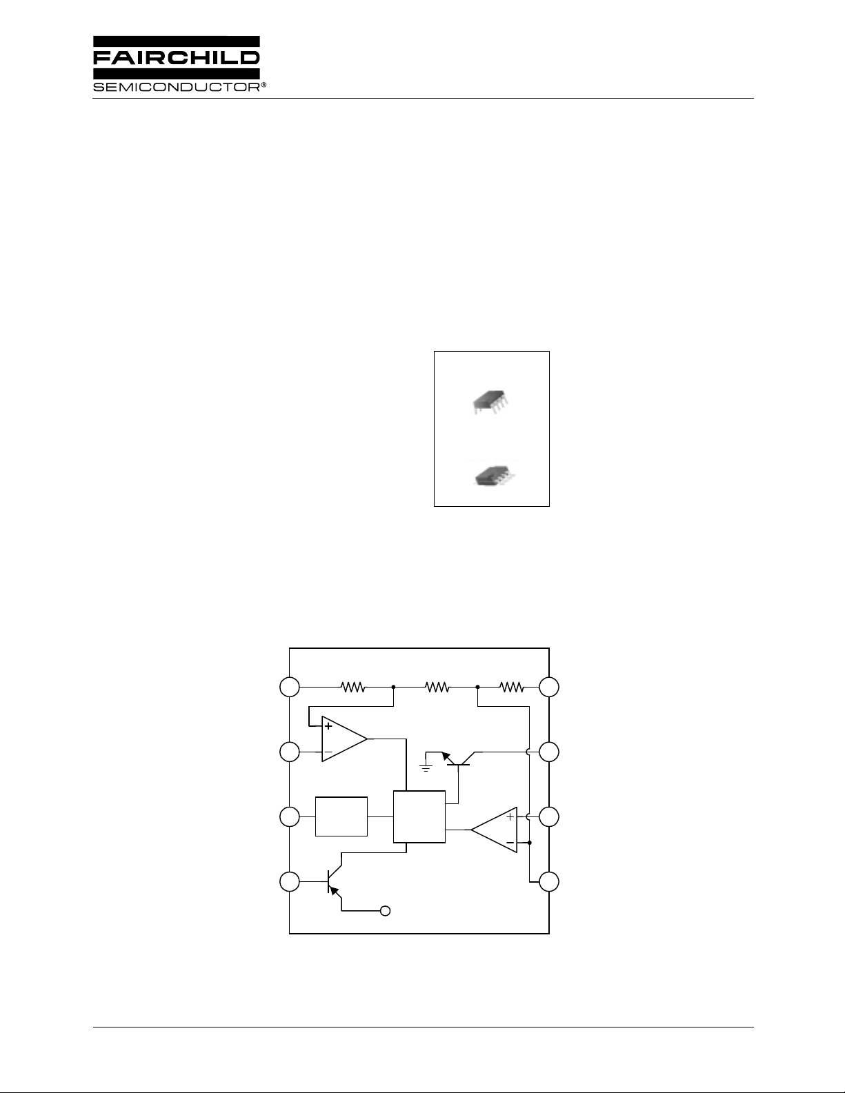
Internal Block Diagram
Internal Block Diagram
Internal Block DiagramInternal Block Diagram
GND
GND
GNDGND
Trigger
Trigger
TriggerTrigger
Output
Output
OutputOutput
Reset
Reset
ResetReset
1
RRRRR
1111
Comp.
Comp.
Comp.Comp.
2222
OutPut
OutPut
OutPutOutPut
3333
Stage
Stage
StageStage
4444
Vref
Vref
VrefVref
RR
RR
Discharging Tr.
Discharging Tr.
Discharging Tr.Discharging Tr.
F/F
F/F
F/FF/F
Comp.
Comp.
Comp.Comp.
R
RR
8888
Vcc
Vcc
VccVcc
7777
Discharge
Discharge
DischargeDischarge
6666
Threshold
Threshold
ThresholdThreshold
Control
Control
ControlControl
5555
Voltage
Voltage
VoltageVoltage
©2002 Fairchild Semiconductor Corporation
Rev. 1.0.3

LM555/NE555/SA555
Absolute Maximum Ratings (T
Absolute Maximum Ratings (T
Absolute Maximum Ratings (TAbsolute Maximum Ratings (T
Parameter
Parameter Symbol
ParameterParameter
Supply Voltage V
Lead Temperature (Soldering 10sec) T
Power Dissipation P
Operating Temperature Range
LM555/NE555
SA555
Storage Temperature Range T
= 25
= 25°°°°C)
= 25 = 25
AAAA
C)
C)C)
Symbol Value
SymbolSymbol
LEAD
T
OPR
STG
CC
D
Value Unit
ValueValue
16 V
300 °C
600 mW
0 ~ +70
-40 ~ +85
-65 ~ +150 °C
Unit
UnitUnit
°C
2222

Electrical Characteristics
Electrical Characteristics
Electrical CharacteristicsElectrical Characteristics
(TA = 25°C, V
Parameter
Parameter Symbol
ParameterParameter
= 5 ~ 15V, unless otherwise specified)
CC
Symbol Conditions
SymbolSymbol
Supply Voltage V
Supply Current (Low Stable) (Note1) I
CC
Timing Error (Monostable)
Initial Accuracy (Note2)
Drift with Temperature (Note4)
Drift with Supply Voltage (Note4)
ACCUR
∆t/∆T
∆t/∆V
CC
LM555/NE555/SA555
Conditions Min.
ConditionsConditions
Min. Typ.
Min.Min.
Typ. Max.
Typ.Typ.
Max. Unit
Max.Max.
-4.5-16V
VCC = 5V, RL = ∞ -36mA
= 15V, RL = ∞ -7.515mA
V
CC
RA = 1kΩ to100kΩ
C = 0.1µF
CC
-1.0
50
0.1
3.0
0.5
Unit
UnitUnit
%
ppm/°C
%/V
Timing Error (Astable)
Intial Accuracy (Note2)
Drift with Temperature (Note4)
Drift with Supply Voltage (Note4)
ACCUR
∆t/∆T
∆t/∆V
Control Voltage V
Threshold Voltage V
Threshold Current (Note3) I
Trigger Voltage V
Trigger Current I
Reset Voltage V
Reset Current I
Low Output Voltage V
High Output Voltage V
Rise Time of Output (Note4) t
Fall Time of Output (Note4) t
Discharge Leakage Current I
C
TH
TH
TR
TR
RST
RST
OL
OH
R
F
LKG
RA = 1kΩ to 100kΩ
C = 0.1µF
CC
-
2.25
150
0.3
VCC = 15V 9.0 10.0 11.0 V
V
= 5V 2.6 3.33 4.0 V
CC
VCC = 15V - 10.0 - V
= 5V - 3.33 - V
V
CC
-----0.10.25 µA
V
= 5V 1.1 1.67 2.2 V
CC
= 15V 4.5 5 5.6 V
V
CC
V
= 0V 0.01 2.0 µA
TR
----0.40.71.0V
----0.10.4mA
VCC = 15V
I
SINK
I
SINK
V
CC
I
SINK
= 10mA
= 50mA
= 5V
= 5mA
-0.06
0.3
-0.050.35 V
VCC = 15V
I
SOURCE
I
SOURCE
V
CC
I
SOURCE
= 200mA
= 100mA 12.75
= 5V
= 100mA
12.5
13.3
2.75 3.3 - V
---- - 100 - ns
---- - 100 - ns
---- - 20 100 nA
-%
ppm/°C
%/V
0.25
0.75
V
V
-V
V
Notes:
Notes:
Notes:Notes:
1. When the output is high, the supply current is typically 1mA less than at V
2. Tested at V
3. This will determine the maximum value of R
total R = 6.7MΩ.
4. These parameters, although guaranteed, are not 100% tested in production.
= 5.0V and V
CC
CC
= 15V.
+ RB for 15V operation, the max. total R = 20MΩ, and for 5V operation, the max.
A
CC
= 5V.
3333

LM555/NE555/SA555
Application Information
Application Information
Application InformationApplication Information
Table 1 below is the basic operating table of 555 timer:
Table 1. Basic Operating Table
Table 1. Basic Operating Table
Table 1. Basic Operating TableTable 1. Basic Operating Table
Threshold Voltage
Threshold Voltage
Threshold Voltage Threshold Voltage
(V
(V
)(PIN 6)
)(PIN 6)
(V(V
)(PIN 6))(PIN 6)
th
th
thth
Trigger Voltage
Trigger Voltage
Trigger VoltageTrigger Voltage
(V
(V
)(PIN 2)
)(PIN 2)
(V(V
)(PIN 2))(PIN 2)
tr
tr
trtr
Reset(PIN 4)
Reset(PIN 4) Output(PIN 3)
Reset(PIN 4)Reset(PIN 4)
Output(PIN 3)
Output(PIN 3)Output(PIN 3)
Discharging Tr.
Discharging Tr.
Discharging Tr.Discharging Tr.
(PIN 7)
(PIN 7)
(PIN 7)(PIN 7)
Don't care Don't care Low Low ON
> 2Vcc / 3 Vth > 2Vcc / 3 High Low ON
V
th
Vcc / 3 < V
< 2 Vcc / 3 Vcc / 3 < Vth < 2 Vcc / 3 High - -
th
< Vcc / 3 Vth < Vcc / 3 High High OFF
V
th
When the low signal input is applied to the reset terminal, the timer output remains low regardless of the threshold voltage or
the trigger voltage. Only when the high signal is applied to the reset terminal, the timer's output changes according to
threshold voltage and trigger voltage.
When the threshold voltage exceeds 2/3 of the supply voltage while the timer output is high, the timer's internal discharge Tr.
turns on, lowering the threshold voltage to below 1/3 of the supply voltage. During this time, the timer output is maintained
low. Later, if a low signal is applied to the trigger voltage so that it becomes 1/3 of the supply voltage, the timer's internal
discharge Tr. turns off, increasing the threshold voltage and driving the timer output again at high.
1. Monostable Operation
1. Monostable Operation
1. Monostable Operation1. Monostable Operation
Trigger
4
RESET
TRIG
2
OUT
3
GND
L
Figure 1. Monoatable Circuit
Figure 1. Monoatable Circuit
Figure 1. Monoatable CircuitFigure 1. Monoatable Circuit
1
8
Vcc
DISCH
THRES
CONT
+Vcc
2222
10
10
R
A
7
6
5
C1
C2R
1010
1111
10
10
1010
R
R
0000
10
10
1010
-1
-1
-1-1
10
10
1010
Capacitance(uF)
Capacitance(uF)Capacitance(uF)
Capacitance(uF)
-2
-2
-2-2
10
10
1010
-3
-3
-3-3
10
10
1010
-5
-5
-5-5
10
10
1010
Figure 2. Resistance and Capacitance vs.
Figure 2. Resistance and Capacitance vs.
Figure 2. Resistance and Capacitance vs.Figure 2. Resistance and Capacitance vs.
RR
-4
-4
-3
-3
-4-4
-3-3
10
10
10
10
1010
1010
Time delay( t
Time delay( t
Time delay( tTime delay(t
Ω
Ω
ΩΩ
=1k
=1k
=1k=1k
A
A
AA
-2
-2
-2-2
10
10
1010
Time Delay(s)
Time Delay(s)
Time Delay(s)Time Delay (s)
Ω
Ω
Ω
ΩΩ
Ω
ΩΩ
10k
10k
10k10k
10
10
1010
))))
dddd
1M
100k
1M
100k
1M1M
100k100 k
-1
-1
0000
-1-1
10
10
1010
Ω
Ω
ΩΩ
Ω
Ω
ΩΩ
10M
10M
10M10M
1111
2222
10
10
10
10
1010
1010
Figure 3. Waveforms of Monostable Operation
Figure 3. Waveforms of Monostable Operation
Figure 3. Waveforms of Monostable OperationFigure 3. Waveforms of Monostable Operation
4444

LM555/NE555/SA555
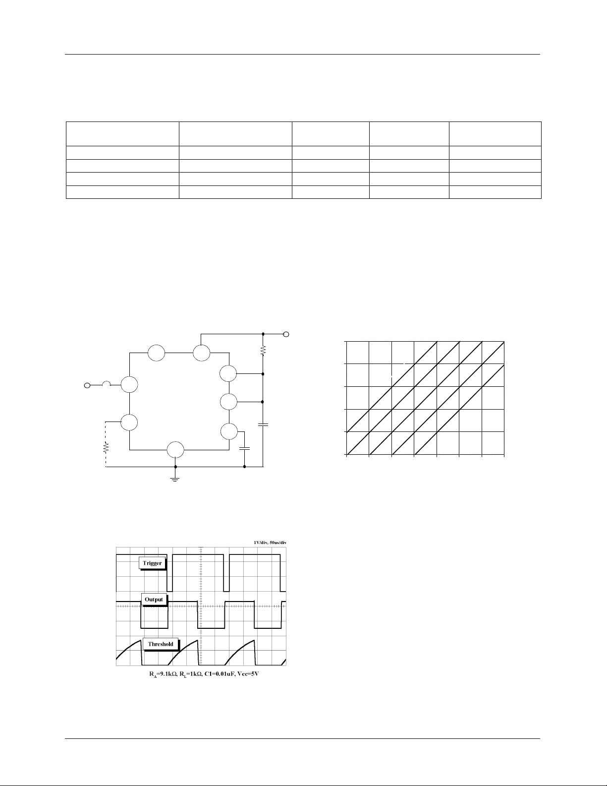
Figure 1 illustrates a monostable circuit. In this mode, the timer generates a fixed pulse whenever the trigger voltage falls
below Vcc/3. When the trigger pulse voltage applied to the #2 pin falls below Vcc/3 while the timer output is low, the timer's
internal flip-flop turns the discharging Tr. off and causes the timer output to become high by charging the external capacitor C1
and setting the flip-flop output at the same time.
The voltage across the external capacitor C1, V
at td=1.1R
for the V
*C. Hence, capacitor C1 is charged through resistor RA. The greater the time constant RAC, the longer it takes
A
to reach 2Vcc/3. In other words, the time constant RAC controls the output pulse width.
C1
increases exponentially with the time constant t=RA*C and reaches 2Vcc/3
C1
When the applied voltage to the capacitor C1 reaches 2Vcc/3, the comparator on the trigger terminal resets the flip-flop,
turning the discharging Tr. on. At this time, C1 begins to discharge and the timer output converts to low.
In this way, the timer operating in the monostable repeats the above process. Figure 2 shows the time constant relationship
based on R
and C. Figure 3 shows the general waveforms during the monostable operation.
A
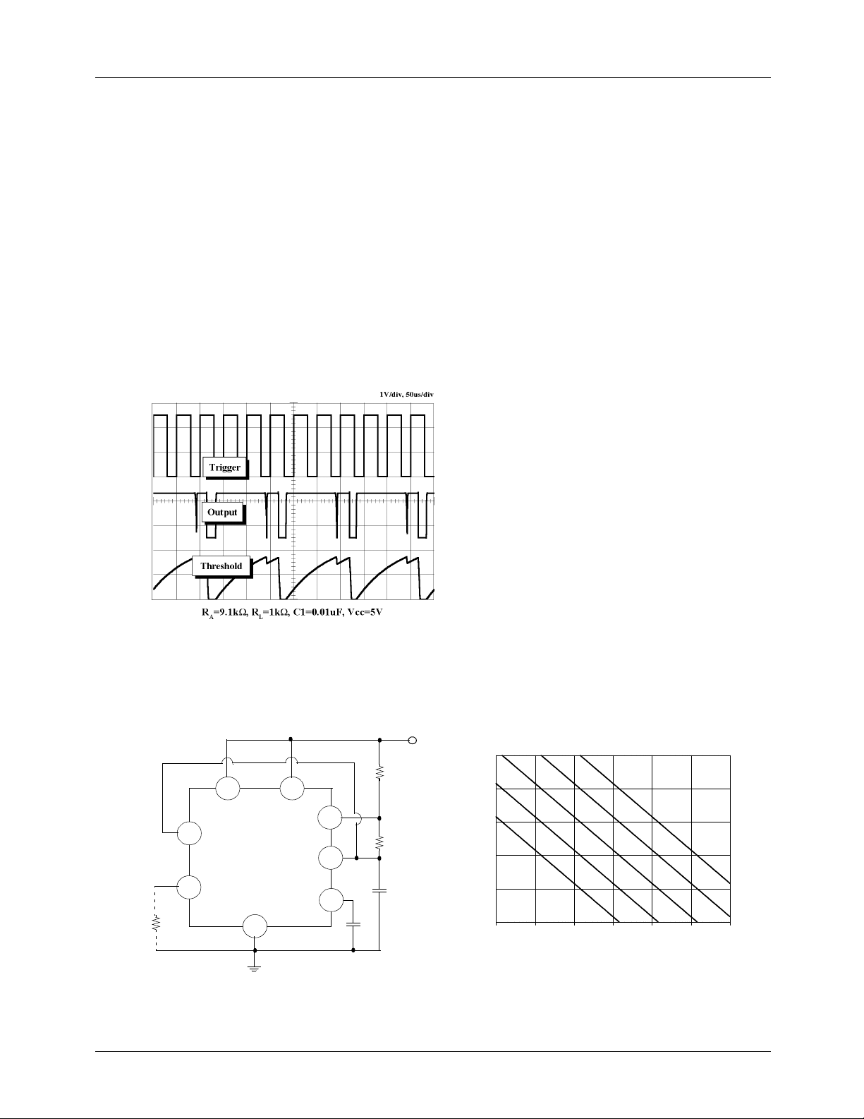
It must be noted that , for a norma l oper ati on, the trig ger pul se vo ltage needs to ma intai n a min imum of Vcc/ 3 befor e the time r
output turns low. That is, alth ough the output remains unaf fected even if a dif f erent trigger pulse is applied while the output is
high, it may be affected and the waveform does not operate properly if the trigger pulse voltage at the end of the output pulse
remains at below Vcc/3. Figure 4 shows such a timer output abnormality.
Figure 4. Waveforms of Monostable Operation (abnormal)
Figure 4. Waveforms of Monostable Operation (abnormal)
Figure 4. Waveforms of Monostable Operation (abnormal)Figure 4. Waveforms of Monostable Operation (abnormal)
2. Astable Operation
2. Astable Operation
2. Astable Operation2. Astable Operation
+Vcc
R
4
RESET
TRIG
2
OUT
3
GND
L
Figure 5. Astable Circuit
Figure 5. Astable Circuit
Figure 5. Astable CircuitFigure 5. Astable Circuit
8
Vcc
DISCH
THRES
1
CONT
7
R
6
5
C2R
A
B
C1
100k
100k
100k100k
Ω
Ω
ΩΩ
1M
1M
1M1M
Ω
Ω
ΩΩ
10 100
1010
Frequency(Hz)
Frequency(Hz)
Frequency(Hz)Frequency(Hz)
1k
1k
1k1k
Ω
Ω
ΩΩ
10k
10k
10k10k
Ω
Ω
ΩΩ
100 1k
100100
(R
(R
+2R
+2R
))))
(R(R
+2R+2R
AAAA
BBBB
1k 10k
1k1k
10k 100k
100k
10k10k
100k100k
100
100
100100
10
10
1010
1111
0.1
0.1
0.10.1
Capacitance(uF)
Capacitance(uF)Capacitance(uF)
Capacitance(uF)
0.01
0.01
0.010.01
1E-3
1E-3
1E-31E-3
100m
100m 111110
100m100m
Figure 6. Capacitance and Resistance vs. Frequency
Figure 6. Capacitance and Resistance vs. Frequency
Figure 6. Capacitance and Resistance vs. FrequencyFigure 6. Capacitance and Resistance vs. Frequency
10M
10M10M
10M
Ω
Ω
ΩΩ
5555
 Loading...