Fairchild LM317AHV service manual

j
查询LM317AHV供应商
LM317AHV
3-Terminal Positive Adjustable Regulator
www.fairchildsemi.com
Features
• Output Current in Excess of 1.5A
• Output Adjustable Between 1. 2V and 57V
• Internal Thermal Overload Protection
• Internal Short Circuit Current Limiting
• Output Transistor Safe Area Compensation
• TO-220 Package
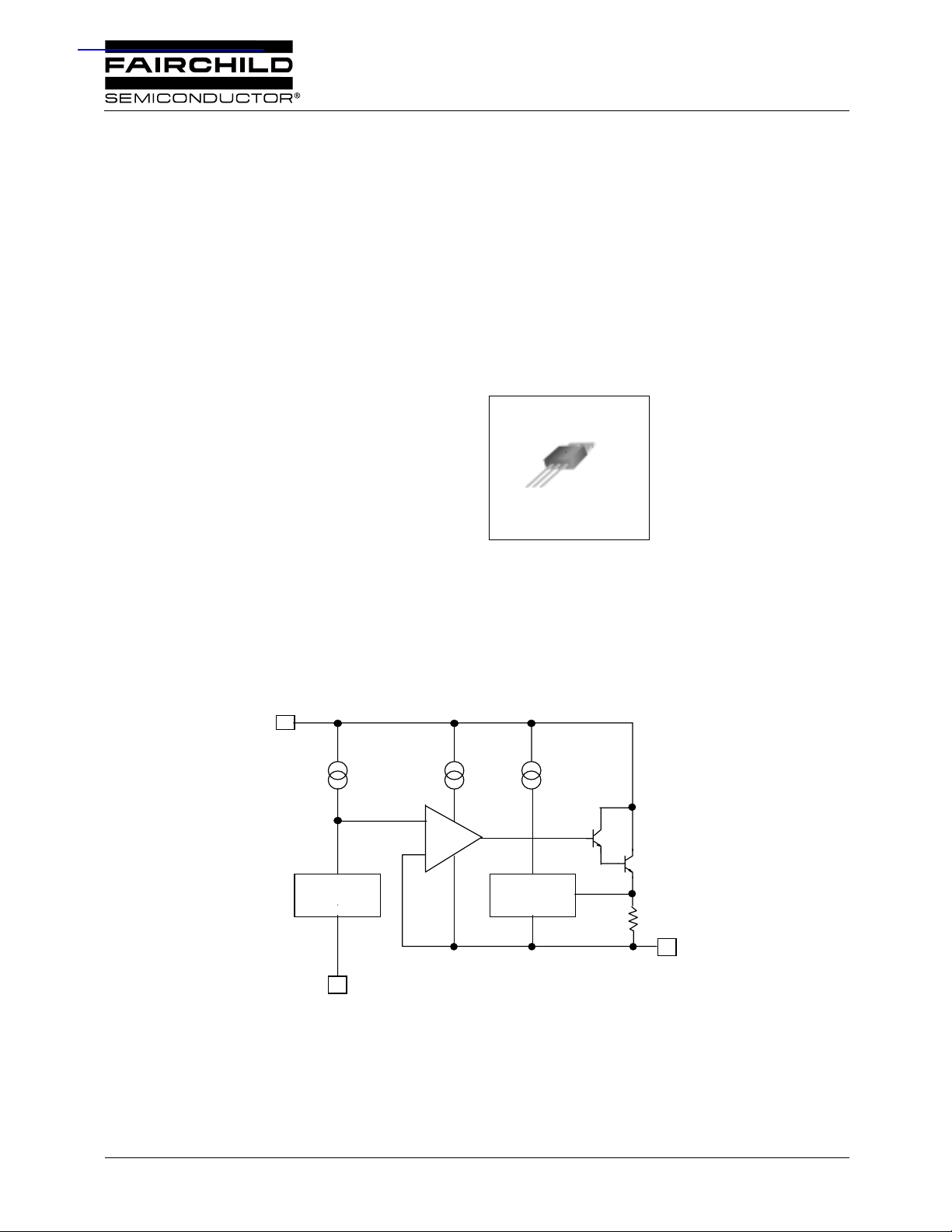
Internal Block Diagram
Description
This monolithic integrated circuit is an adjustable 3-terminal
positive voltage regulator designed to supply more than 1.5A
of load current with an output voltage adjustable over a 1.2
to 57V. It employs internal current limiting, thermal shut
down and safe area compensation.
TO-220
1
1. Adj 2. Output 3. Input
Output
3
2
3Vin
Input
Voltage
Reference
©2002 Fairchild Semiconductor Corporation
Vad
+
-
Protection
Circuitry
Rlimit
2
Vo
Output
1
Rev. 1.0.1

LM317AHV
Absolute Maximum Ratings
Parameter Symbol Value Unit
Input-Output Voltage Differential V
Lead Temperature T
Power Dissipation P
Operating Junction Temperature Range T
Storage Temperature Range T
- V
I
LEAD
D
j
STG
O
60 V
230 °C
Internally limited W
0 ~ +125 °C
-65 ~ +125 °C
Temperature Coefficient of Output Voltage ∆Vo/∆T ±0.02 %/°C
Electrical Characteristics
(VI-VO=5V, IO= 0.5A, 0°C ≤ TJ ≤ + 125°C, I
Parameter Symbol Conditions Min. Typ. Max. Unit
Line Regulation (Note1) Rline
Load Regulation (Note1) Rload
Adjustable Pin Current I
Adjustable Pin Current Change ∆I
Reference Voltage V
Temperature Stability ST
Minimum Load Current to Maintain
Regulation
Maximum Output Current I
RMS Noise, % of V
OUT
Ripple Rejection RR
Long-Term Stability, T
= T
J
HIGH
Thermal Resistance Junction to Case R
= 1.5A, P
MAX
ADJ
ADJ
REF
T
I
L(MIN)VI
O(MAX)
e
N
ST
θJC
= 20W, unless otherwise specified)
DMAX
T
= +25°C
A
3V ≤ V
3V ≤ V
T
- V
≤ 60V
I
O
- V
≤ 60V - 0.02 0.07 %/V
I
O
= +25°C, 10mA ≤I
A
VO< 5V
V
≥ 5V
O
10mA ≤ I
O
≤ I
MAX
VO < 5V
V
5V
O ≥
O ≤IMAX
- 0.01 0.04 %/V
-18
0.4250.5
%/V
-40
0.8701.5
%/V
- - 46 100 µA
3V ≤ VI - V
10mA ≤ I
PD ≤ P
3V ≤ VIN - V
10mA ≤ I
P
≤ P
D
O
MAX
O
MAX
O
≤ I
≤ I
≤60V
MAX
≤60V
O
MAX
-2.05 µA
1.20 1.25 1.30 V
--0.7-%/V
- VO = 60V - 3.5 12 mA
VI - V
VI - V
T
= 25°C
A
O
O
≤ 15V, PD ≤ P
≤ 60V, PD ≤ P
MAX
MAX
1.0
2.2
0.3
-A
TA= +25°C, 10Hz ≤ f ≤ 10kHz - 0.003 0.01 %/V
= 10V, f = 120Hz
V
O
without C
C
ADJ
T
A
ADJ
= 10µF (Note2)
= +25°C for end point
measurements, 1000HR
66 60
-dB
75
-0.31 %
- -5-°C/W
mV
O
mV
O
O
O
Note :
1. Load and line regulation are specified at constant junction temperature. Change in V
into account separately. Pulse testing with low duty is used. (P
2. C
, when used, is connected between the adjustment pin and ground.
ADJ
MAX
= 20W)
2
due to heatin g effe cts must be tak en
D
 Loading...