Fairchild LM317 service manual

现货库存、技术资料、百科信息、热点资讯,精彩尽在鼎好!
LM317
3-Terminal Positive Adjustable Regulator
LM317 3-Terminal Positive Adjustable Regulator
March 2000
Revised June 2005
General Description
This monolithic integrated circuit is an adjustable 3-terminal
positive voltage regulator designed to supply more than
1.5A of load current wit h an output v oltage a djustabl e over
a 1.2 to 37V. It employs internal current limiting, thermal
shut-down and safe area compensation.
Features
■ Output Current In Excess of 1.5A
■ Output Adjustable Between 1.2V and 37V
■ Internal Thermal Overload Protection
■ Internal Short Circuit Current Limiting
■ Output Transistor Safe Operating Area Compen satio n
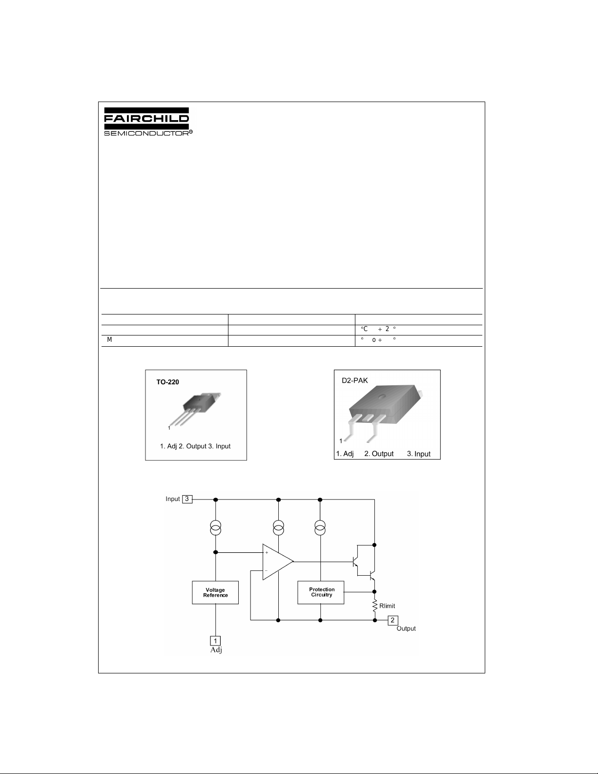
■ TO-220 Package
■ D2 PAK Package
Ordering Code:
Product Number Package Operating Temperature
LM317T TO-220 0
LM317D2TXM D2 PAK 0
Connection Diagrams
Internal Block Diagram
q
C to 125qC
q
C to 125qC
© 2005 Fairchild Semiconductor Corporation DS400281 www.fairchildsemi.com

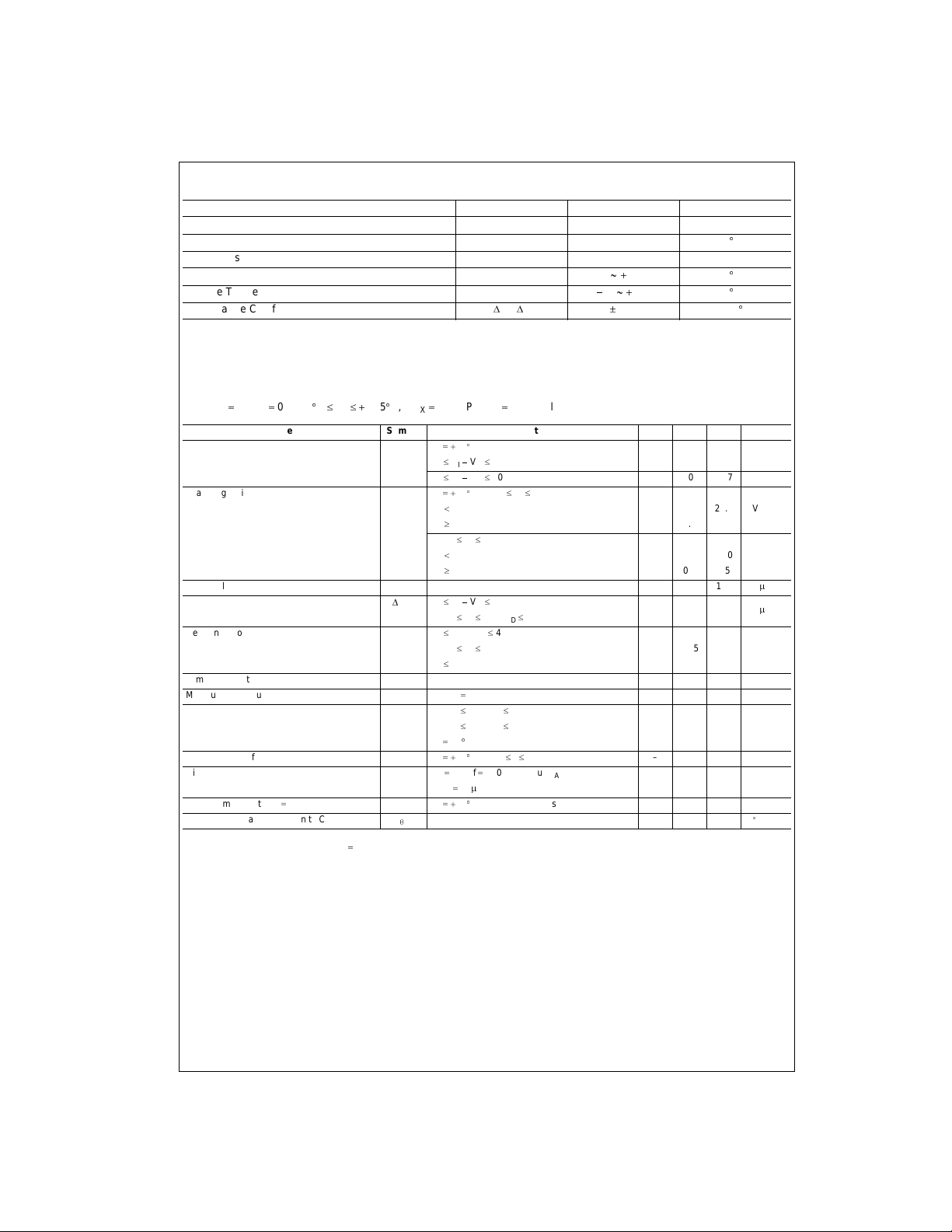
Absolute Maximum Ratings
LM317
Input-Output Voltage Differential V
Lead Temperature T
Power Dissipation P
Operating Junction Temperature Range T
Storage Temperature Range T
Temperature Coefficient of Output Voltage
Note 1: Absolute Maximum Rating s: are those values beyond which the safety of the devic e canno t be guara nteed. T he device should no t be oper ated at
these limits. The parametric values defined in the Electr ic al C haracteristics tables are not gu aranteed at the absolute m ax im um ratings. The “Recommended
Operating Cond iti ons” table will define the c onditions for actual device operation.
Parameter Symbol Value Unit
- V
I
LEAD
'
VO/'T
O
D
j
STG
40 V
230
Internally limited W
0 a 125
65 a 125
r
0.02 % / qC
Electrical Characteristic
(VI - VO 5V, IO 0.5A, 0qC d TJ d 125qC, I
Parameter Symbol Conditions Min Typ Max Unit
Line Regulation (Note 2) Rline T
Load Regulation (Note 2) Rload TA 25qc, 10mA d IO d I
Adjustable Pin Current I
Adjustable Pin Current Change
Reference Voltage V
Temperature Stability ST
Minimum Load Current to Maintain Regulation I
Maximum Output Current I
RMS Noise,% of V
Ripple Rejection RR VO 10V, f 120Hz without C
Long-Term Stability, TJ T
Thermal Resistance Junction to Case R
Note 2: Load and line re gulation are specif ied at constant junc t ion temperature. C hange in VD due to heating effec ts must be taken int o account separately.
Pulse testing with low duty is used. (P
Note 3: CADJ, when used, is c onnected between th e adjustment pin and ground.
OUT
HIGH
MAX
20S)
1.5A, P
MAX
25qC
A
3V d VI VO d 40V
3V d VI VO d 40V – 0.02 0.07 % / V
VO 5V – 18.0 25.0 mV% / V
VO t 5V 0.4 0.5
10mA d IO d I
VO 5V – 40.0 70.0 mV% / V
VO t 5V 0.8 1.5
ADJ
'
I
3V d VI VO d 40V
ADJ
10mA d IO d I
3V d VIN - VO d 40V
REF
PD d P
T
- VO 40V – 3.5 12.0 mA
L(MIN)VI
O(MAX)VI
- VO d 15V, PD d P
- VO d 40V, PD d P
I
TA 25qC
eN TA 25qC, 10Hz d f d 10KHz – 0.003 0.01 % / V
C
10PF (Note 3) 75.0
ADJ
ST TA 25qC for end point measurements, 1000HR – 0.3 1.0 %
T
JC
20W, unless otherwise specified)
DMAX
MAX
MAX
––46.0 100
d P
MAX PD
MAX
MAX
MAX
––0.7 – % / V
MAX
MAX
ADJ
––5.0 –qC / W
–– 0.01 0.04 % / V
– 2.0 5.0
1.20 1.25 1.30 V10mA d IO d I
1.0 2.2
0.3 –
66.0 60.0 –
q
C
q
C
q
C
O
O
P
A
P
A
O
AV
O
dB
www.fairchildsemi.com 2
 Loading...