Fairchild FST3257 service manual

FST3257
Quad 2:1 Multiplexer / Demultiplexer Bus Switch
FST3257 — Quad 2:1 Multiplexer / Demultiplexer Bus Switch
May 2009
Features
4Ω Switch Connection Between Two Ports
Minimal Propagation Delay Through the Switch
Low I
CC
Zero Bounce in Flow-Through Node
Control Inputs Compatible with TTL Level
Description
The Fairchild Switch FST3257 is a quad 2:1 high-speed
CMOS TTL-compatible multiplexer / demultiplexer bus
switch. The low on resistance of the switch allows
inputs to be connected to outputs without adding
propagation delay or generating additional ground
bounce noise.
When /OE is LOW , the select pin connects the A port to
the selected B port output. When /OE is HIGH, the
switch is OPEN and a high-impedance state exists
between the two ports.
Ordering Information
Operating
Part Number
Temperature
Eco Status
Package
Range
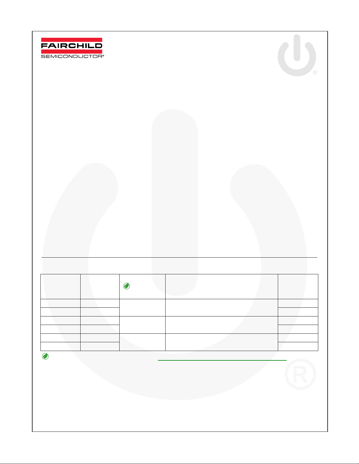
FST3257M -40 to 85°C Tubes
FST3257MX -40 to 85°C
FST3257QSC -40 to 85°C Tubes
FST3257QSCX -40 to 85°C
FST3257MTC -40 to 85°C Tubes
FST3257MTCX -40 to 85°C
RoHS
Green
RoHS
16-Lead Small Outline Integrated Circuit
(SOIC) JEDEC MS-012,0.150 Narrow
16-Lead Quarter Size Outline Package
(QSOP) JEDEC MO-137 0.150 Inch Wide
16-Lead Thin Shrink Small Outline Package
(TSSOP) JEDEC MO-153, 4mm Wide
Packing
Method
Tape and Reel
Tape and Reel
Tape and Reel
For Fairchild’s definition of Eco Status, please visit: http://www.fairchildsemi.com/company/green/rohs_green.html.
© 1997 Fairchild Semiconductor Corporation www.fairchildsemi.com
FST3257 • Rev. 1.0.3

Pin Assignments
FST3257 — Quad 2:1 Multiplexer / Demultiplexer Bus Switch
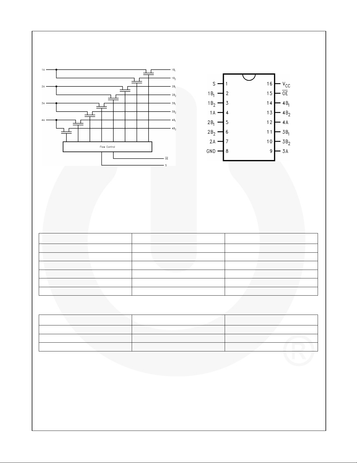
Figure 1. Logic Diagram
Pin Descriptions
Pin # Names Description
1 S Select Input
2, 3, 5, 6, 10, 11, 13, 14 1B1, 1B
4, 7, 9, 12 1A, 2A, 3A, 4A Bus A
8 GND Ground
15 /OE Bus Switch Enables
16 VCC Supply Voltage
Truth Table
Select Inputs Bus Switch Enabled Function
S Logic Level HIGH Disconnected
Logic Level LOW Logic Level LOW A=B1
Logic Level HIGH Logic Level LOW A=B2
Figure 2. Connection Diagram
, 2B2, 3B1, 3B2, 4B1, 4B2 Bus B
2 ,2B1
© 1997 Fairchild Semiconductor Corporation www.fairchildsemi.com
FST3257 • Rev. 1.0.3 2

FST3257 — Quad 2:1 Multiplexer / Demultiplexer Bus Switch
Absolute Maximum Ratings
Stresses exceeding the absolute maximum ratings may damage the device. The device may not function or be
operable above the recommended operating conditions and stressing the parts to these levels is not recommended.
In addition, extended exposure to stresses above the recommended operating conditions may affect device
reliability. The absolute maximum ratings are stress ratings only.
Symbol Parameter Min. Max. Unit
VCC Supply Voltage -0.5 +7.0 V
VS DC Switch Voltage -0.5 +7.0 V
VIN DC Input Voltage
IIK DC Input Current -50 mA
I
DC Output Sink Current 128 mA
OUT
ICC/I
DC VCC/GND Current ±100 mA
GND
T
Storage Temperature Range -65 +150 °C
STG
Note:
1. The input and output negative voltage ratings may be exceeded if the input and output diode current ratings are
observed.
(1)
-0.5 +7.0 V
Recommended Operating Conditions
The Recommended Operating Conditions table defines the conditions for actual device operation. Recommended
operating conditions are specified to ensure optimal performance to the datasheet specifications. Fairchild does not
recommend exceeding them or designing to Absolute Maximum Ratings.
Symbol Parameter Min. Max. Unit
VCC Power Supply Operating 3.0 5.5 V
VIN Input Voltage 0 5.5 V
V
Output Voltage 0 5.5 V
OUT
tr,tf Input Rise and Fall Time
TA Free Air Operating Temperature -40 +85 °C
Note:
2. Unused control inputs must be held HIGH or LOW. They may not float.
Switch Control Input 0 5
Switch I/O 0 DC
ns/V
© 1997 Fairchild Semiconductor Corporation www.fairchildsemi.com
FST3257 • Rev. 1.0.3 3
 Loading...