Fairchild FST3245 service manual

FST3245 — 8-Bit Bus Switch
FST3245 — 8-Bit Bus Switch
March 2008
Features
4Ω Switch Connection between Two Ports
Minimal Propagation Delay through the Switch
Low I
CC
Zero Bounce in Flow-through Mode
Control Inputs Compatible with TTL Level
Description
The FST3245 switch provides eight-bits of high-speed
CMOS TTL-compatible bus switching in a standard ’245
pin-out. The low on resistance allows inputs to be
connected to outputs without adding propagation delay
or generating additional ground bounce noise.
The device is organized as an eight-bit switch. When
/OE is LOW, the switch is ON and port A is connected
to port B. When /OE is HIGH, the switch is OPEN and a
high-impedance state exists between the two ports.
Ordering Information
Operating
Part Number
Temperature
Package
Range
FST3245WMX
FST3245QSC
FST3245QSCX
FST3245MTC
FST3245MTCX
All packages are lead free per JEDEC: J-STD-020B standard.
The Fairchild switch fami l y deri ves from and embodies Fairchild ’ s proven switch technology used for several years in its
74LVX3L384 (FST3384) bus switch product.
-40 to +85°C
-40 to +85°C
-40 to +85°C
-40 to +85°C
-40 to +85°C
20-Lead, Small Outline Integrated Circuit (SOIC), JEDEC
MS-013, 0.300-inch Wide
20-Lead Quarter Size Outline Package (QSOP), JEDEC
MO-137, 0.150-inch Wide
20-Lead Quarter Size Outline Package (QSOP),
JEDEC MO-137, 0.150-inch Wide
20-Lead Thin Shrink Small Outline Package (TSSOP),
JEDEC MO-153, 4.4mm Wide
20-Lead Thin Shrink Small Outline Package (TSSOP),
JEDEC MO-153, 4.4mm Wide
Packing
Method
Tape and Reel
Tape and Reel
Tape and Reel
Tube
Tube
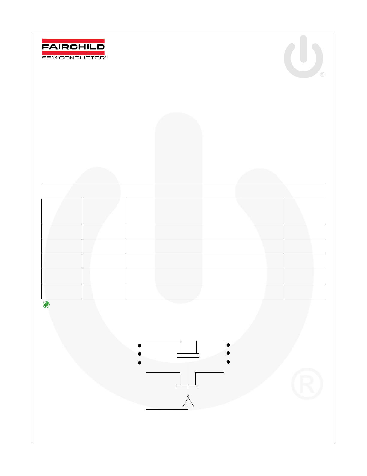
Logic Diagram
2
A
0
9
A
7
19
/OE
Figure 1. Logic Diagram
©1997 Fairchild Semiconductor Corporation www.fairchildsemi.com
FST3245 • Rev. 1.0.2
18
11
B
0
B
7

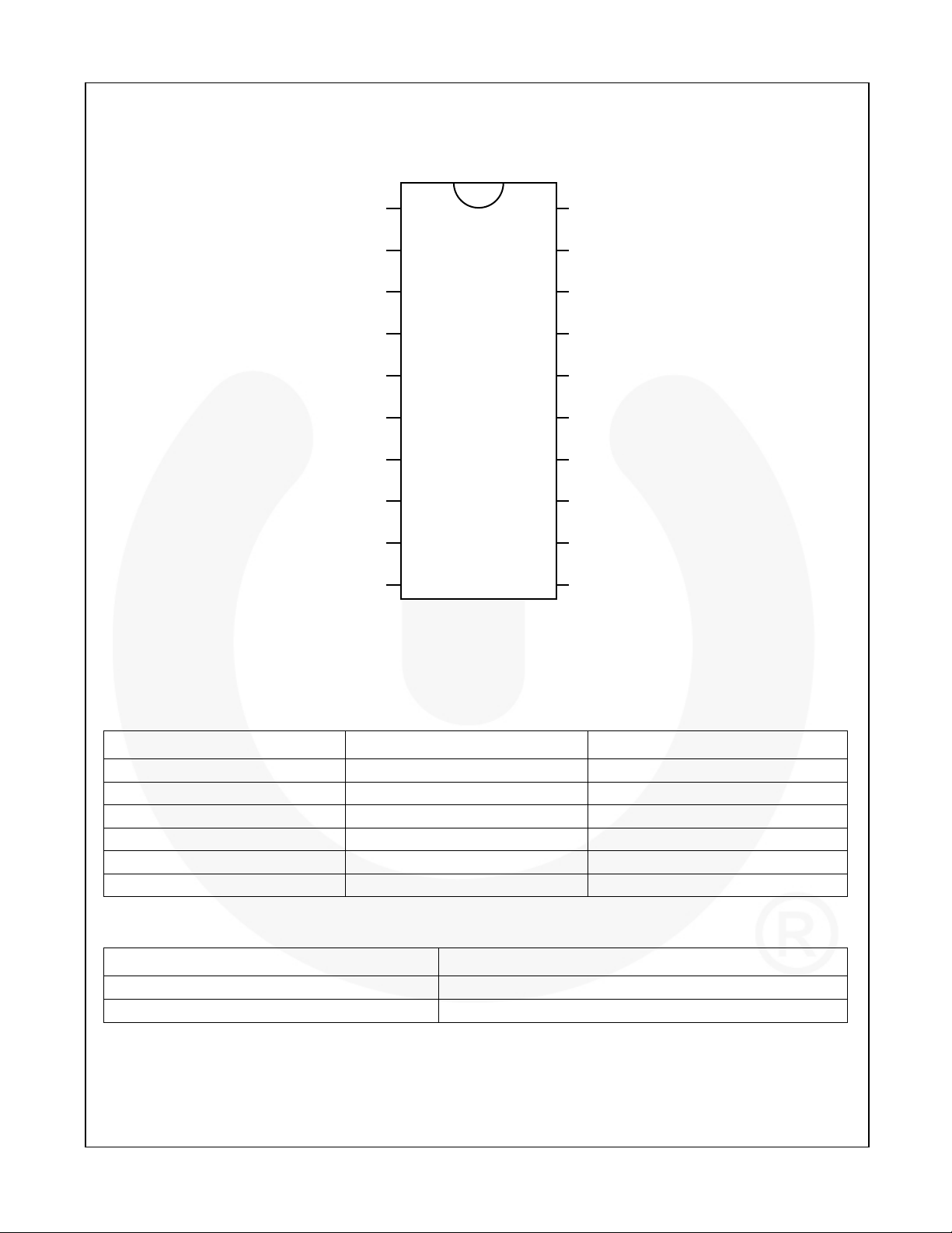
Pin Configuration
FST3245 — 8-Bit Bus Switch
NC
A
A
A
A
A
A
A
A
GND
1
2
0
3
1
4
2
5
3
6
4
7
5
8
6
9
7
10 11
Figure 2. Pin Configuration
20
19
18
17
16
15
14
13
12
V
CC
/OE
B
0
B
1
B
2
B
3
B
4
B
5
B
6
B
7
Pin Descriptions
Pin # Pin Names Description
1 NC No Connnect
19 /OE Bus Switch Enable
2,3,4,5,6,7,8,9 A0,A1,A2,A3,A4,A5,A6,A7 Bus A
10 GND Ground
11,12,13,14,15,16,17,18 B7,B6,B5,B4,B3,B2,B1,B0 Bus B
20 VCC Supply Voltage
Truth Table
Input /OE
LOW Connect
HIGH Disconnect
Function
© 1997 Fairchild Semiconductor Corporation www.fairchildsemi.com
FST3245 • Rev. 1.0.2 2

FST3245 — 8-Bit Bus Switch
Absolute Maximum Ratings
Stresses exceeding the absolute maximum ratings may damage the device. The device may not function or be
operable above the recommended operating conditions and stressing the parts to these levels is not recommended.
In addition, extended exposure to stresses above the recommended operating conditions may affect device
reliability. The absolute maximum ratings are stress ratings only.
Symbol Parameter Min. Max. Unit
VCC Supply Voltage -0.5 7.0 V
VS DC Switch Voltage -0.5 7.0 V
VIN DC Input Voltage
IIK DC Input Diode Current, V
I
DC Output Sink Current 128 mA
OUT
I
/ I
CC
DC V
GND
T
Storage Temperature Range -65 +150 °C
STG
/ GND Current ±100 mA
CC
Note:
1. The input and output negative voltage ratings may be exceeded if the input and output diode current ratings are
observed.
(1)
-0.5 7.0 V
< 0V -50 mA
IN
Recommended Operating Conditions
The Recommended Operating Conditions table defines the conditions for actual device operation. Recommended
operating conditions are specified to ensure optimal performance to the datasheet specifications. Fairchild does not
recommend exceeding them or designing to Absolute Maximum Ratings.
Symbol Parameter Min. Max. Unit
VCC Power Supply Operating 4.0 5.5 V
VIN Input Voltage 0 5.5 V
V
Output Voltage 0 5.5 V
OUT
tr, tf Input Rise and Fall Time
Switch Control Input
Switch I/O 0 DC
TA Operating Temperature, Free Air -40 +85 °C
Note:
2. Unused control inputs must be held HIGH or LOW. They may not float.
(2)
0 5
ns/V
© 1997 Fairchild Semiconductor Corporation www.fairchildsemi.com
FST3245 • Rev. 1.0.2 3
 Loading...