

Fairchild FSD156MRBN service manual

FSD156MRBN
Green-Mode Fairchild Power Switch (FPS™)
FSD156MRBN — Green-Mode Fairchild Power Switch (FPS™)
October 2011
Features
Advanced Soft Burst-Mode Operation for
Low Standby Power and Low Audible Noise
Random Frequency Fluctuation (RFF) for Low EMI
Pulse-by-Pulse Current Limit
Various Protection Functions: Overload Protection
(OLP), Over-Voltage Protection (OVP), Abnormal
Over-Current Protection (AOCP), Internal Thermal
Shutdown (TSD) with Hysteresis, Output-Short
Protection (OSP), and Under-Voltage Lockout
(UVLO) with Hysteresis
Low Operating Current (0.4mA) in Burst Mode
Internal Startup Circuit
Internal High-Voltage SenseFET: 650V
Built-in Soft-Start: 15ms
Auto-Restart Mode
Applications
Power Supply for LCD Monitor, STB, and DVD
Combination
Description
The FSD156MRBN is an integrated Pulse Width
Modulation (PWM) controller and SenseFET specifically
designed for offline Switch-Mode Power Supplies
(SMPS) with minimal external components. The PWM
controller includes an integrated fixed-frequency
oscillator, Under-Voltage Lockout (UVLO), LeadingEdge Blanking (LEB), optimized gate driver, internal
soft-start, temperature-compensated precise current
sources for loop compensation, and self-protection
circuitry. Compared with a discrete MOSFET and PWM
controller solution, the FSD series can reduce total cost,
component count, size, and weight; while
simultaneously increasing efficiency, productivity, and
system reliability. This device provides a basic platform
suited for cost-effective design of a flyback converter.
Ordering Information
(2)
Output Power Table
Operating
Part Number Package
Junction
Temperature
FSD156MRBN 8-DIP
Notes:
1. Lead-free package per JEDEC J-STD-020B.
2. The junction temperature can limit the maximum output power.
3. 230V
4. Typical continuous power in a non-ventilated enclosed adapter measured at 50C ambient temperature.
5. Maximum practical continuous power in an open-frame design at 50C ambient temperature.
© 2011 Fairchild Semiconductor Corporation www.fairchildsemi.com
FSD156MRBN • Rev. 1.0.0
or 100/115VAC with voltage doubler.
AC
-40°C ~
+125°C
Current
Limit
1.60A
R
DS(ON)
(Max.)
2.3
230VAC ±15%
Adapter
(4)
26W 40W 20W 30W
(3)
Open
Frame
Adapter
(5)
85-265V
(4)
Frame
AC
Open
Replaces
Device
(5)
FSFM300N
FSGM300
Application Circuit
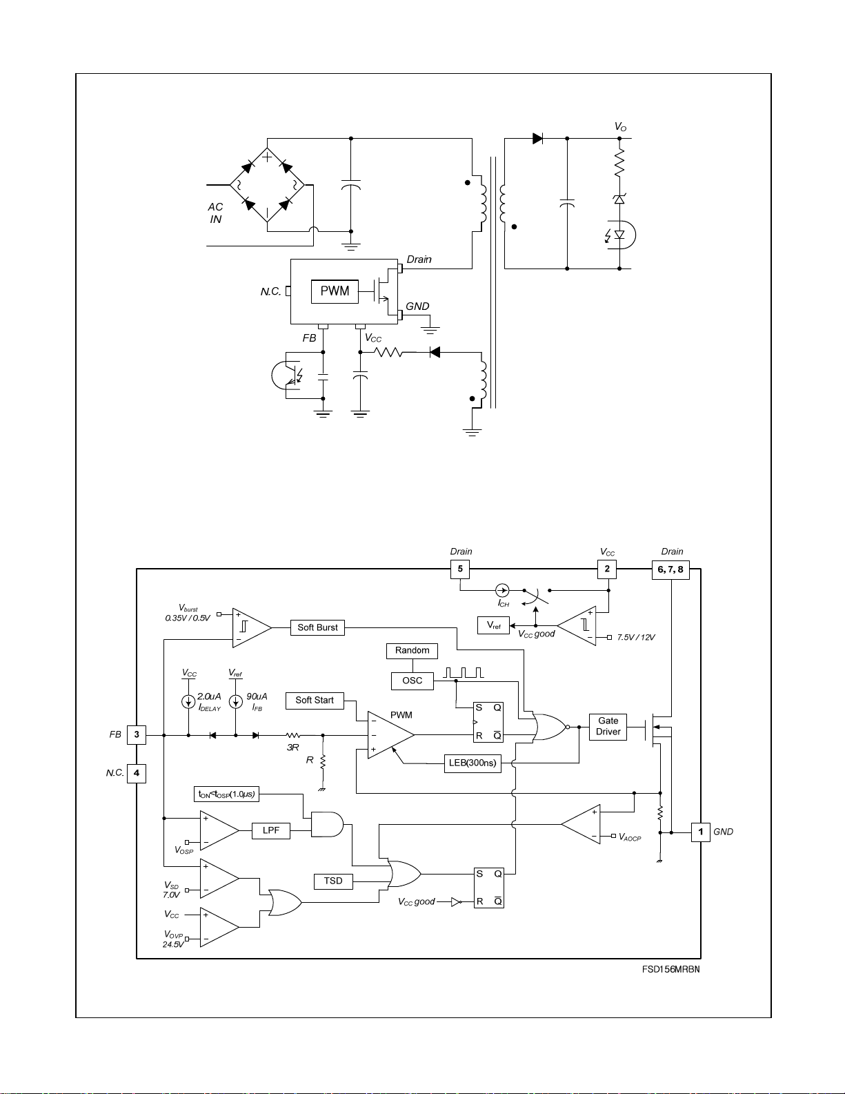
FSD156MRBN — Green-Mode Fairchild Power Switch (FPS™)
Figure 1. Typical Application Circuit
Internal Block Diagram
Figure 2. Internal Block Diagram
© 2011 Fairchild Semiconductor Corporation www.fairchildsemi.com
FSD156MRBN • Rev. 1.0.0 2
Pin Configuration
FSD156MRBN — Green-Mode Fairchild Power Switch (FPS™)
1. GND
2. V
CC
FSD156MRBN
3. FB
4. N.C.
Figure 3. Pin Configuration (Top View)
Pin Definitions
Pin # Name Description
1 GND
2 VCC
3 FB
4 NC
5, 6, 7, 8 Drain
Ground. This pin is the control ground and the SenseFET source.
Power Supply. This pin is the positive supply input, which provides the internal operating
current for both startup and steady-state operation.
Feedback. This pin is internally connected to the inverting input of the PWM comparator.
The collector of an opto-coupler is typically tied to this pin. For stable operation, a capacitor
should be placed between this pin and GND. If the voltage of this pin reaches 7.0V, the
overload protection triggers, which shuts down the FPS™.
No Connection
SenseFET Drain. High-voltage power SenseFET drain connection.
8. Drain
7. Drain
6. Drain
5. Drain
© 2011 Fairchild Semiconductor Corporation www.fairchildsemi.com
FSD156MRBN • Rev. 1.0.0 3

FSD156MRBN — Green-Mode Fairchild Power Switch (FPS™)
Absolute Maximum Ratings
Stresses exceeding the absolute maximum ratings may damage the device. The device may not function or be
operable above the recommended operating conditions and stressing the parts to these levels is not recommended.
In addition, extended exposure to stresses above the recommended operating conditions may affect device reliability.
The absolute maximum ratings are stress ratings only.
Symbol Parameter Min. Max. Unit
V
Drain Pin Voltage 650 V
DS
V
V
CC
V
Feedback Pin Voltage
FB
I
Drain Current Pulsed 4 A
DM
I
Continuous Switching Drain Current
DS
EAS Single Pulsed Avalanche Energy
PD
T
J
T
Storage Temperature
STG
ESD
Notes:
6. Repetitive peak switching current when the inductive load is assumed: Limited by maximum duty (D
and junction temperature (see Figure 4).
7. L=45mH, starting T
8. Infinite cooling condition (refer to the SEMI G30-88).
9. Although this parameter guarantees IC operation, it does not guarantee all electrical characteristics.
Pin Voltage 26 V
CC
Total Power Dissipation (TC=25C)
-0.3
T
=25C
(6)
C
TC=100C
(7)
190 mJ
(8)
1.9 A
1.27 A
1.5 W
10.0 V
Maximum Junction Temperature 150
Operating Junction Temperature
Electrostatic
Discharge Capability
=25C.
J
Human Body Model, JESD22-A114 5
Charged Device Model, JESD22-C101 2
(9)
-40
-55
+125
+150
MAX
C
C
C
kV
=0.73)
Figure 4. Repetitive Peak Switching Current
Thermal Impedance
TA=25°C unless otherwise specified.
Symbol Parameter Value Unit
JA Junction-to-Ambient Thermal Impedance
JL Junction-to-Lead Thermal Impedance
Notes:
10. JEDEC recommended environment, JESD51-2, and test board, JESD51-10, with minimum land pattern.
11. Measured on the SOURCE pin #7, close to the plastic interface.
© 2011 Fairchild Semiconductor Corporation www.fairchildsemi.com
FSD156MRBN • Rev. 1.0.0 4
(10)
85 °C/W
(11)
11 °C/W
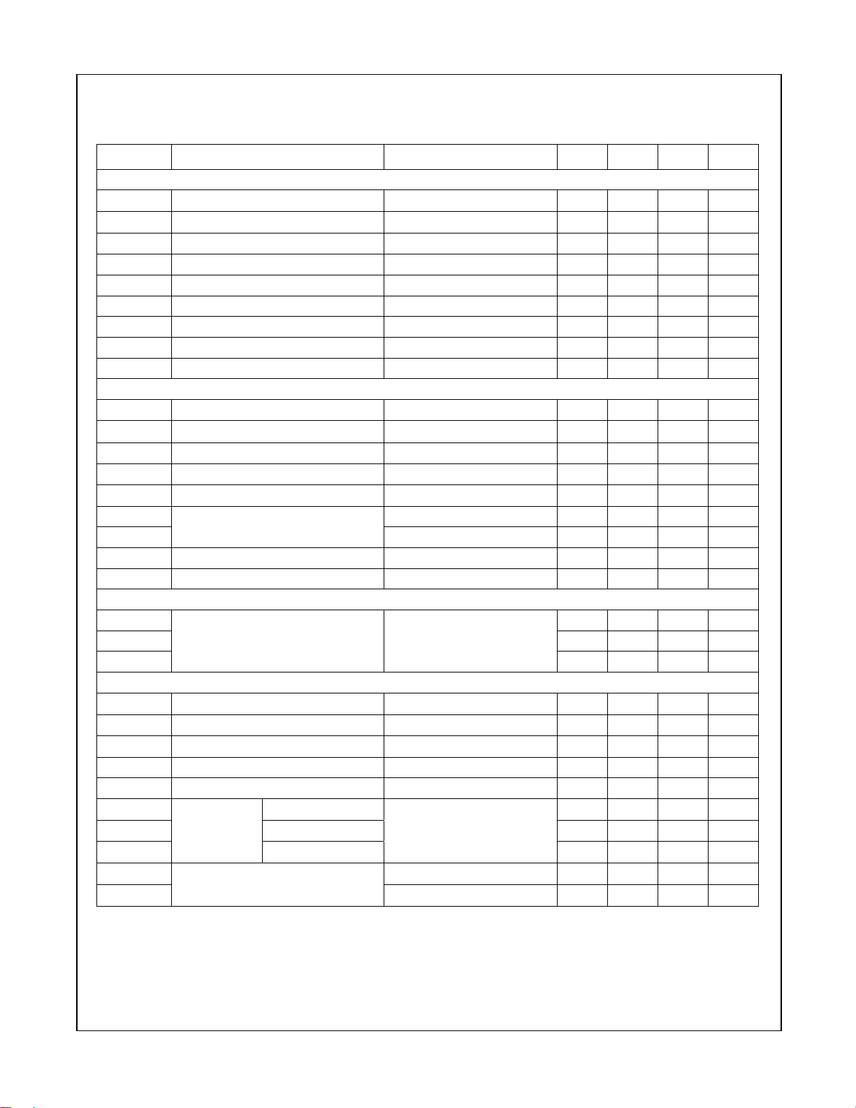
FSD156MRBN — Green-Mode Fairchild Power Switch (FPS™)
Electrical Characteristics
TJ = 25C unless otherwise specified.
Symbol Parameter Conditions Min. Typ. Max. Unit
SenseFET Section
BV
Drain-Source Breakdown Voltage
DSS
I
Zero-Gate-Voltage Drain Current
DSS
R
Drain-Source On-State Resistance VGS=10V, ID =1A 1.8 2.2
DS(ON)
C
Input Capacitance
ISS
C
Output Capacitance
OSS
(12)
V
(12)
V
tr Rise Time V
tf Fall Time V
t
Turn-On Delay V
d(on)
t
Turn-Off Delay V
d(off)
V
= 0V, ID = 250A
CC
V
= 650V, TA = 25C
DS
= 25V, V
DS
= 25V, V
DS
= 325V, ID = 4A, RG=25 26 ns
DS
= 325V, ID = 4A, RG=25 25 ns
DS
= 325V, ID = 4A, RG=25 14 ns
DS
= 325V, ID= 4A, RG=25 32 ns
DS
= 0V, f=1MHz 515 pF
GS
= 0V, f=1MHz 75 pF
GS
Control Section
f
Switching Frequency
S
f
D
MAX
D
MIN
Switching Frequency Variation
S
Maximum Duty Ratio V
Minimum Duty Ratio V
IFB Feedback Source Current V
V
START
V
STOP
t
V
RECOMM
SS
UVLO Threshold Voltage
After Turn-on, V
Internal Soft-Start Time V
Recommended VCC Range 13 23 V
(12)
V
(12)
= 14V, V
CC
-25C < T
= 14V, V
CC
= 14V, V
CC
= 0 65 90 115
FB
V
= 0V, V
FB
= 40V, V
STR
= 4V 61 67 73 kHz
FB
< 125C
J
= 4V 61 67 73 %
FB
= 0V 0 %
FB
Sweep 11 12 13 V
CC
= 0V 7.0 7.5 8.0 V
FB
Sweep 15 ms
CC
Burst-Mode Section
V
BURH
V
BURL
Burst-Mode Voltage V
0.30 0.35 0.40 V
= 14V, VFB Sweep
CC
Hys 150 mV
Protection Section
I
Peak Drain Current Limit
LIM
V
Shutdown Feedback Voltage V
SD
I
Shutdown Delay Current V
DELAY
t
Leading-Edge Blanking Time
LEB
V
Over-Voltage Protection VCC Sweep 23.0 24.5 26.0 V
OVP
t
OSP
V
OSP
t
OSP_FB
TSD
T
HYS
Output-Short
Threshold VFB 1.8 2.0 2.2 V
Protection
V
Thermal Shutdown Temperature
Hysteresis 60
Threshold Time
(12)
FB
Blanking Time 2.0 2.5 3.0
(12,14)
di/dt = 300mA/s
= 14V, V
CC
= 14V, V
CC
Sweep 6.45 7.00 7.55 V
FB
= 4V 1.2 2.0 2.8
FB
300 ns
OSP Triggered when
t
(Lasts Longer than t
Shutdown Temperature 125 135 145
(12)
ON<tOSP
& VFB>V
OSP
OSP_FB
650 V
250
±5 ±10 %
0.45 0.50 0.55 V
1.45 1.60 1.75 A
0.7 1.0 1.3
)
Continued on the following page…
A
A
A
s
s
C
C
© 2011 Fairchild Semiconductor Corporation www.fairchildsemi.com
FSD156MRBN • Rev. 1.0.0 5
 Loading...