Fairchild FSCQ1265RT Service Manual

FSCQ-Series Green Mode Fairchild Power Switch (FPS™)
February 2006
FSCQ-Series
FSCQ0565RT/FSCQ0765RT/FSCQ0965RT/FSCQ1265RT/
FSCQ1465RT/FSCQ1565RT/FSCQ1565RP
Green Mode Fairchild Power Switch (FPS™)
Features
■
Optimized for Quasi-Resonant Converter (QRC)
Advanced Burst-Mode Operation for under 1W
■
Standby Power Consumption
■
Pulse-by-Pulse Current Limit
Over Load Protection (OLP) – Auto Restart
■
■
Over Voltage Protection (OVP) – Auto Restart
Abnormal Over Current Protection (AOCP) – Latch
■
■
Internal Thermal Shutdown (TSD) – Latch
Under Voltage Lock Out (UVLO) with Hysteresis
■
■
Low Startup Current (typical: 25µA)
■
Internal High Voltage SenseFET
Built-in Soft Start (20ms)
■
■
Extended Quasi-Resonant Switching
Applications
CTV
■
■
Audio Amplifier
Related Application Notes
■
AN4146: Design Guidelines for Quasi-Resonant
Converters Using FSCQ-Series Fairchild Power
Switch.
■
AN4140: Transformer Design Consideration for
Off-Line Flyback Converters Using Fairchild Power
Switch.
Description
A Quasi-Resonant Converter (QRC) typically shows
lower EMI and higher power conversion efficiency compared to conventional hard-switched converter with a
fixed switching frequency. Therefore, a QRC is well
suited for noise-sensitive applications, such as color TV
and audio. Each product in the FSCQ-Series contains an
integrated Pulse Width Modulation (PWM) controller and
a SenseFET, and is specifically designed for quasiresonant off-line Switch Mode Power Supplies (SMPS)
with minimal external components. The PWM controller
includes an integrated fixed frequency oscillator, under voltage lockout, leading edge blanking (LEB), optimized gate
driver, internal soft star t, temperature-compensated precise current sources for a loop compensation, and self
protection circuitry. Compared with a discrete MOSFET
and PWM controller solution, the FSCQ-Series can
reduce total cost, component count, size, and weight, while
simultaneously increasing efficiency, productivity, and system reliability . These devices provide a basic platform that
is well suited for cost-effective designs of quasi-resonant
switching flyback converters.
Ordering Information
Product Number Package Marking Code BVdss R
FSCQ0565RTYDTU TO-220F-5L (Forming) CQ0565RT 650V 2.2 Ω
FSCQ0765RTYDTU TO-220F-5L (Forming) CQ0765RT 650V 1.6 Ω
FSCQ0965RTYDTU TO-220F-5L (Forming) CQ0965RT 650V 1.2 Ω
FSCQ1265RTYDTU TO-220F-5L (Forming) CQ1265RT 650V 0.9 Ω
FSCQ1465RTYDTU TO-220F-5L( Forming) CQ1465RT 650V 0.8 Ω
FSCQ1565RTYDTU TO-220F-5L (Forming) CQ1565RT 650V 0.7 Ω
FSCQ1565RPVDTU TO-3PF-7L (Forming) CQ1565RP 650V 0.7 Ω
YDTU: Forming Type
VDTU: Forming Type
©2006 Fairchild Semiconductor Corporation
FSCQ-Series Rev. 1.1.2
Max.
ds(ON)
1
www.fairchildsemi.com
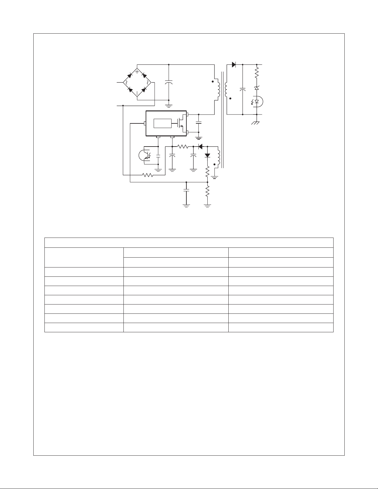
Typical Circuit
FSCQ-Series Green Mode Fairchild Power Switch (FPS™)
V
O
AC
IN
Drain
GND
Sync
FSCQ-Series
PWM
V
FB
V
CC
Figure 1. Typical Flyback Application
Table 1. Maximum Output Power
Output Power Table
230 V AC ± 15%
Product
FSCQ0565RT 70W 60W
FSCQ0765RT 100W 85W
FSCQ0965RT 130W 110W
FSCQ1265RT 170W 140W
FSCQ1465RT 190W 160W
FSCQ1565RT 210W 170W
FSCQ1565RP 250W 210W
Notes:
1. Maximum practical continuous power in an open frame design at 50 ° C ambient.
2. 230 VAC or 100/115 VAC with doubler.
3. The junction
emperature can limit the
t
maximum output power.
Open Frame
2
1
3
85–265 V AC
Open Frame
1
FSCQ-Series Rev. 1.1.2
2
www.fairchildsemi.com
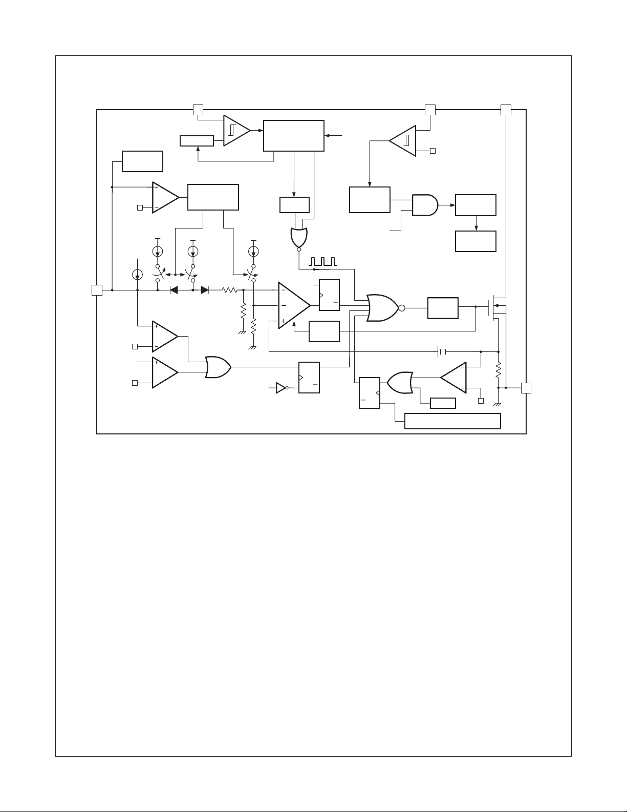
Internal Block Diagram
FSCQ-Series Green Mode Fairchild Power Switch (FPS™)
Sync
5
+
Threshold
Soft Start
V
Burst
Normal Operation
Vref
I
BFB
V
CC
I
delay
V
4
FB
V
SD
Sync
Vovp
Vref
-
4.6V/2.6V: Normal QR
3.0V/1.8V: Extended QR
Burst Mode
Controller
Burst Switching
I
FB
2.5R
R
VCC good
(V
CC
Vref
= 9V)
Quasi-Resonant
(QR) Switching
Controller
OSC
I
B
PWM
SQQ
R
SQQ
R
LEB
600ns
fs
Auxiliary
V
CC
Vref
Normal
Operation
SQQ
R
good
Vcc Drain
3 1
+
-
9V/15V
Main Bias
Internal
Bias
Gate
Driver
AOCP
TSD
Power Off Reset (VCC = 6V)
Vocp
2
GND
Figure 2. Functional Block Diagram of FSCQ-Series
FSCQ-Series Rev. 1.1.2
3
www.fairchildsemi.com

Pin Configuration
FSCQ-Series Green Mode Fairchild Power Switch (FPS™)
TO-220F-5L
5. Sync
4. Vfb
3. Vcc
2. GND
1. Drain
TO-3PF-7L
5. Sync
4. Vfb
3. Vcc
2. GND
1. Drain
Figure 3. Pin Configuration (Top View)
Pin Definitions
Pin Number Pin Name Pin Function Description
1Drain High voltage power SenseFET drain connection.
2 GND This pin is the control ground and the SenseFET source.
3 Vcc This pin is the positive supply input. This pin provides internal operating current for
both start-up and steady-state operation.
4 Vfb This pin is internally connected to the inverting input of the PWM comparator.
The collector of an optocoupler is typically tied to this pin. For stable operation,
a capacitor should be placed between this pin and GND. If the voltage of this
pin reaches 7.5V, the over load protection triggers
shutting down.
5 Sync This pin is internally connected to the sync detect comparator for quasi-resonant
switching. In normal quasi-resonant operation, the threshold of the sync
comparator is 4.6V/2.6V. Whereas, the sync threshold is changed to 3.0V/1.8V
in an extended quasi-resonant operation.
,
which results in the FPS
FSCQ-Series Rev. 1.1.2
4
www.fairchildsemi.com

Absolute Maximum Ratings
(T
= 25°C, unless otherwise specified)
A
Parameter Symbol Value Unit
Drain Pin Voltage V
Supply V oltage V
Analog Input Voltage Range V
Drain Current Pulsed
4
I
FSCQ0565RT 11.2 A
DM
FSCQ0765RT 15.2
FSCQ0965RT 16.4
FSCQ1265RT 21.2
FSCQ1465RT 22
FSCQ1565RT 26.4
FSCQ1565RP 33.2
Continuous Drain Current (Tc = 25 ° C)
(Tc: Case Back Surface Temperature)
FSCQ0565RT 2.8 A
I
D
FSCQ0765RT 3.8
FSCQ0965RT 4.1
FSCQ1265RT 5.3
FSCQ1465RT 5.5
FSCQ1565RT 6.6
FSCQ1565RP 8.3
Continuous Drain Current* (T
(T
Drain Lead Temperature)
DL:
DL
= 25 ° C)
I
* FSCQ0565RT 5 A
D
FSCQ0765RT 7
FSCQ0965RT 7.6
FSCQ1265RT 11
FSCQ1465RT 12
FSCQ1565RT 13.3
FSCQ1565RP 15
Continuous Drain Current (T
= 100 ° C) I
C
FSCQ0565RT 1.7 A
D
FSCQ0765RT 2.4
FSCQ0965RT 2.6
FSCQ1265RT 3.4
FSCQ1465RT 3.5
FSCQ1565RT 4.4
FSCQ1565RP 5.5
Single-Pulsed Avalanche Energy
5
E
FSCQ0565RT 400 mJ
AS
FSCQ0765RT 570
FSCQ0965RT 630
FSCQ1265RT 950
FSCQ1465RT 1000
FSCQ1565RT 1050
FSCQ1565RP 1050
sync
V
DS
CC
FB
650 V
20 V
-0.3 to 13V V
-0.3 to V
CC
(rms)
(rms)
(rms)
FSCQ-Series Green Mode Fairchild Power Switch (FPS™)
V
FSCQ-Series Rev. 1.1.2
5
www.fairchildsemi.com

°
°
°
°
FSCQ-Series Green Mode Fairchild Power Switch (FPS™)
Absolute Maximum Ratings
(T
= 25°C, unless otherwise specified)
A
Total Power Dissipation
(Tc = 25 ° C with Infinite Heat Sink)
(Continued)
P
FSCQ0565RT 38 W
D
FSCQ0765RT 45
FSCQ0965RT 49
FSCQ1265RT 50
FSCQ1465RT 60
FSCQ1565RT 75
FSCQ1565RP 98
Operating Junction Temperature T
Operating Ambient Temperature T
Storage Temperature Range T
J
A
STG
+150
-25 to +85
-55 to +150
ESD Capability, HBM Model (All pins except Vfb) – 2.0
(GND – Vfb = 1.7kV)
ESD Capability, Machine Model (All pins except Vfb) – 300
(GND – Vfb = 170V)
Notes:
4. Repetitive rating: pulse width limited by maximum junction temperature.
5. L = 15mH, starting T
= 25 ° C, These parameters, although guaranteed at the design, are not tested in mass production.
j
C
C
C
kV
V
Thermal Impedance
(T
= 25°C unless otherwise specified)
A
Parameter Symbol Value Unit
Junction to Case Thermal Impedance
θ
JC
FSCQ0565RT 3.29
FSCQ0765RT 2.60
FSCQ0965RT 2.55
FSCQ1265RT 2.50
FSCQ1465RT 2.10
FSCQ1565RT 2.00
FSCQ1565RP 1.28
C/W
FSCQ-Series Rev. 1.1.2
6
www.fairchildsemi.com

Electrical Characteristics (SenseFET Part)
(T
= 25°C unless otherwise specified)
A
Parameter Symbol Condition Min. Typ. Max. Unit
Drain-Source Breakdown Voltage BV
Zero Gate Voltage Drain Current I
Drain-Source ON-State
DSS
R
Resistance
Input Capacitance C
Output Capacitance C
DSS
DS(ON)
ISS
OSS
FSCQ0565RT V
FSCQ0765RT V
FSCQ0965RT V
FSCQ1265RT V
FSCQ1465RT V
FSCQ1565RT V
FSCQ1565RP V
FSCQ0565RT V
FSCQ0765RT – 1415 –
FSCQ0965RT – 1750 –
FSCQ1265RT – 2400 –
FSCQ1465RT – 2400 –
FSCQ1565RT – 3050 –
FSCQ1565RP – 3050 –
FSCQ0565RT V
FSCQ0765RT – 100 –
FSCQ0965RT – 130 –
FSCQ1265RT – 175 –
FSCQ1465RT – 185 –
FSCQ1565RT – 220 –
FSCQ1565RP – 220 –
V
= 0V, I
GS
V
= 650V,V
DS
= 10V, I
GS
= 10V, I
GS
= 10V, I
GS
= 10V, I
GS
= 10V, I
GS
= 10V, ID = 1A – 0.53 0.7
GS
= 10V, ID = 1A – 0.53 0.7
GS
= 0V, V
GS
= 250 µ A 650 – – V
D
= 0V – – 250 µ A
GS
= 1A – 1.76 2.2
D
= 1A – 1.4 1.6
D
= 1A – 1.0 1.2
D
= 1A – 0.75 0.9
D
= 1A – 0.7 0.8
D
DS
= 25V,
– 1080 – pF
f = 1MHz
GS
= 0V, V
DS
= 25V,
–90– pF
f = 1MHz
Ω
FSCQ-Series Green Mode Fairchild Power Switch (FPS™)
FSCQ-Series Rev. 1.1.2
7
www.fairchildsemi.com

Electrical Characteristics (Continued)
(TA = 25°C unless otherwise specified)
Parameter Symbol Condition Min. Typ. Max. Unit
Control Section
V
Switching Frequency F
Switching Frequency Variation
7
∆F
Feedback Source Current I
Maximum Duty Cycle D
Minimum Duty Cycle D
UVLO Threshold V oltage V
V
Soft Start Time
6
OSC
OSC
FB
MAX
MIN
START
STOP
T
SS
= 5V, V
FB
-25°C ≤ TA ≤ 85°C0±5 ±10 %
V
= 0.8V, V
FB
V
= 5V, V
FB
V
= 0V, V
FB
V
= 1V 14 15 16 V
FB
Burst Mode Section
Burst Mode Enable Feedback Voltage V
Burst Mode Feedback Source Current I
Burst Mode Switching Time T
Burst Mode Hold Time T
BEN
BFB
BS
BH
VFB = 0V 60 100 140 µA
VFB = 0.9V, Duty = 50% 1.2 1.4 1.6 ms
VFB = 0.9V → 0V 1.2 1.4 1.6 ms
Protection Section
V
Shutdown Feedback Voltage V
Shutdown Delay Current I
Over V oltage Protection V
Over Current Latch Voltage
Thermal Shutdown Temp
Notes:
6. These parameters, although guaranteed, are tested only in EDS (wafer test) process.
7. These parameters, although guaranteed at the design, are not tested in mass production.
6
7
SD
DELAY
OVP
V
OCL
T
SD
= 18V 7.0 7.5 8.0 V
CC
V
= 5V, V
FB
V
= 3V 11 12 13 V
FB
V
= 18V 0.9 1.0 1.1 V
CC
= 18V 18 20 22 kHz
CC
= 18V 0.5 0.65 0.8 mA
CC
= 18V 92 95 98 %
CC
= 18V – 0 – %
CC
8910
18 20 22 ms
0.25 0.40 0.55 V
= 18V 4 5 6 µA
CC
140 – – °C
FSCQ-Series Green Mode Fairchild Power Switch (FPS™)
FSCQ-Series Rev. 1.1.2
8 www.fairchildsemi.com

Electrical Characteristics (Continued)
(TA = 25°C unless otherwise specified)
Parameter Symbol Condition Min. Typ. Max. Unit
Sync Section
Sync Threshold in Normal QR (H) V
Sync Threshold in Normal QR (L) V
Sync Threshold in Extended QR (H) V
Sync Threshold in Extended QR (L) V
Extended QR Enable Frequency F
Extended QR Disable Frequency F
Total Device Section
Operating Supply Current
9
- In Normal Operation I
- In Burst Mode (Non-switching) I
Startup Current I
Sustain Latch Current
11
Current Sense Section
Maximum Current Limit
10
Burst Peak Current I
SH1
SL1
SH2
SL2
SYH
SYL
OP
OB
START
I
SN
I
LIM
BUR(pk)
FSCQ0565RT VFB = 5V – 4 6 mA
FSCQ0765RT – 4 6
FSCQ0965RT – 6 8
FSCQ1265RT – 6 8
FSCQ1465RT – 7 9
FSCQ1565RT – 7 9
FSCQ1565RP – 7 9
FSCQ0565RT VCC = 18V, V
FSCQ0765RT 4.4 5 5.6
FSCQ0965RT 5.28 6.0 6.72
FSCQ1265RT 6.16 7 7.84
FSCQ1465RT 7.04 8.0 8.96
FSCQ1565RT 7.04 8 8.96
FSCQ1565RP 10.12 11.5 12.88
FSCQ0565RT VCC = 18V, V
FSCQ0765RT 0.65 0.9 1.15
FSCQ0965RT 0.6 0.9 1.2
FSCQ1265RT 0.8 1.2 1.6
FSCQ1465RT 0.6 0.9 1.2
FSCQ1565RT – 1 –
FSCQ1565RP – 1 –
VCC = 18V, VFB = 5V 4.2 4.6 5.0 V
2.3 2.6 2.9 V
2.7 3.0 3.3 V
1.6 1.8 2.0 V
–90–kHz
–45–kHz
VFB = GND – 0.25 0.50 mA
V
= V
CC
V
= V
CC
– 0.1V – 25 50 µA
START
– 0.1V – 50 100 µA
STOP
= 5V 3.08 3.5 3.92 A
FB
= Pulse 0.45 0.65 0.85 A
FB
FSCQ-Series Green Mode Fairchild Power Switch (FPS™)
Notes:
9. This parameter is the current flowing in the control IC.
10. These parameters indicate inductor current.
11. These parameters, although guaranteed, are tested only in EDS (wafer test) process.
9 www.fairchildsemi.com
FSCQ-Series Rev. 1.1.2
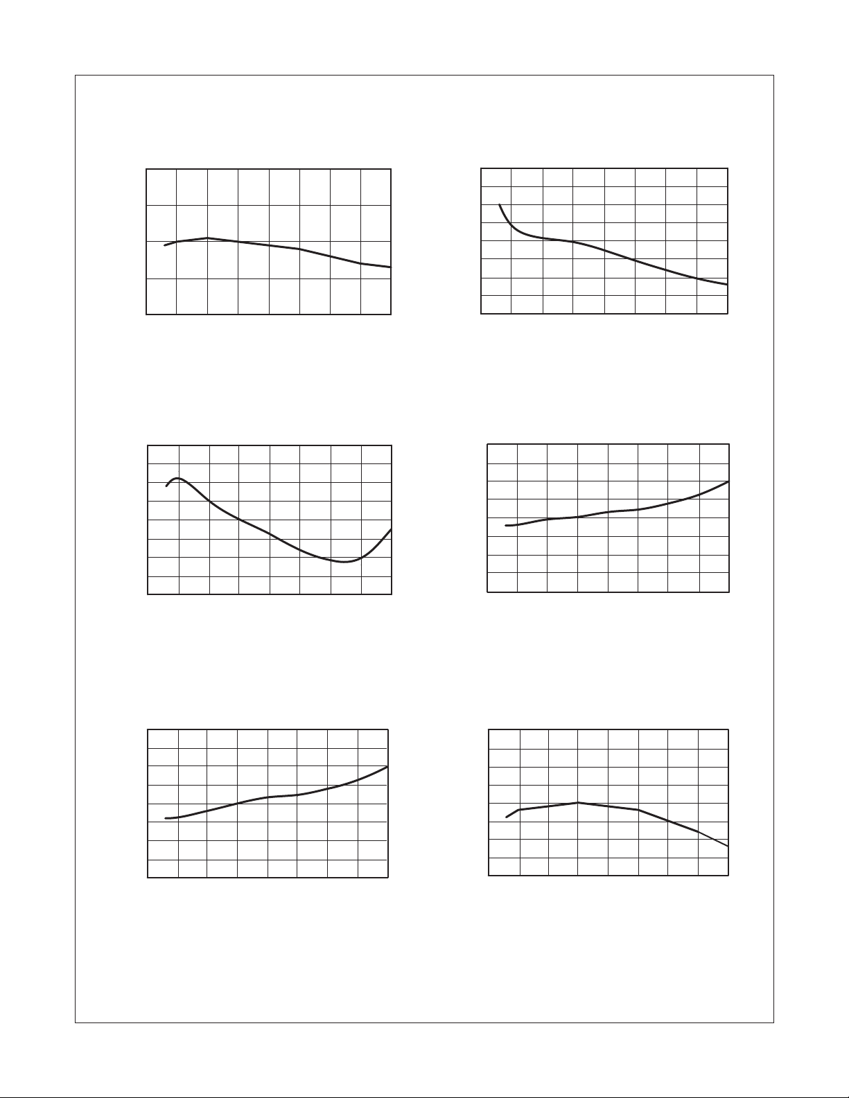
Electrical Characteristics
FSCQ-Series Green Mode Fairchild Power Switch (FPS™)
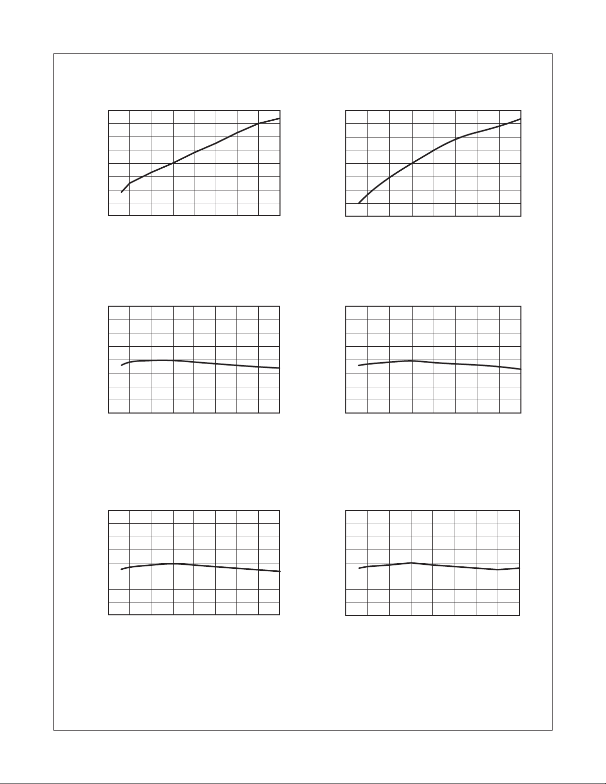
Operating Supply Current
1.2
1.0
Normalized to 25°CNormalized to 25°C
0.8
-50 0 50 100 150
Temp (°C)
Start-Up Current Start Threshold Voltage
1.4
1.2
1.0
Burst-mode Supply Current (Non-Switching)
1.4
1.2
1.0
0.8
Normalized to 25°C
0.6
-50 0 50 100 150
Temp (°C)
1.10
1.05
1.00
0.8
0.6
-50 0 50 100 150
Temp (°C)
Stop Threshold Voltage Initial Frequency
1.10
1.05
1.00
0.95
Normalized to 25°C
0.90
-50 0 50 100 150
Temp (°C)
0.95
Normalized to 25°C
0.90
-50 0 50 100 150
Temp (°C)
1.10
1.05
1.00
0.95
Normalized to 25°C
0.90
-50 0 50 100 150
Temp (°C)
FSCQ-Series Rev. 1.1.2
10 www.fairchildsemi.com
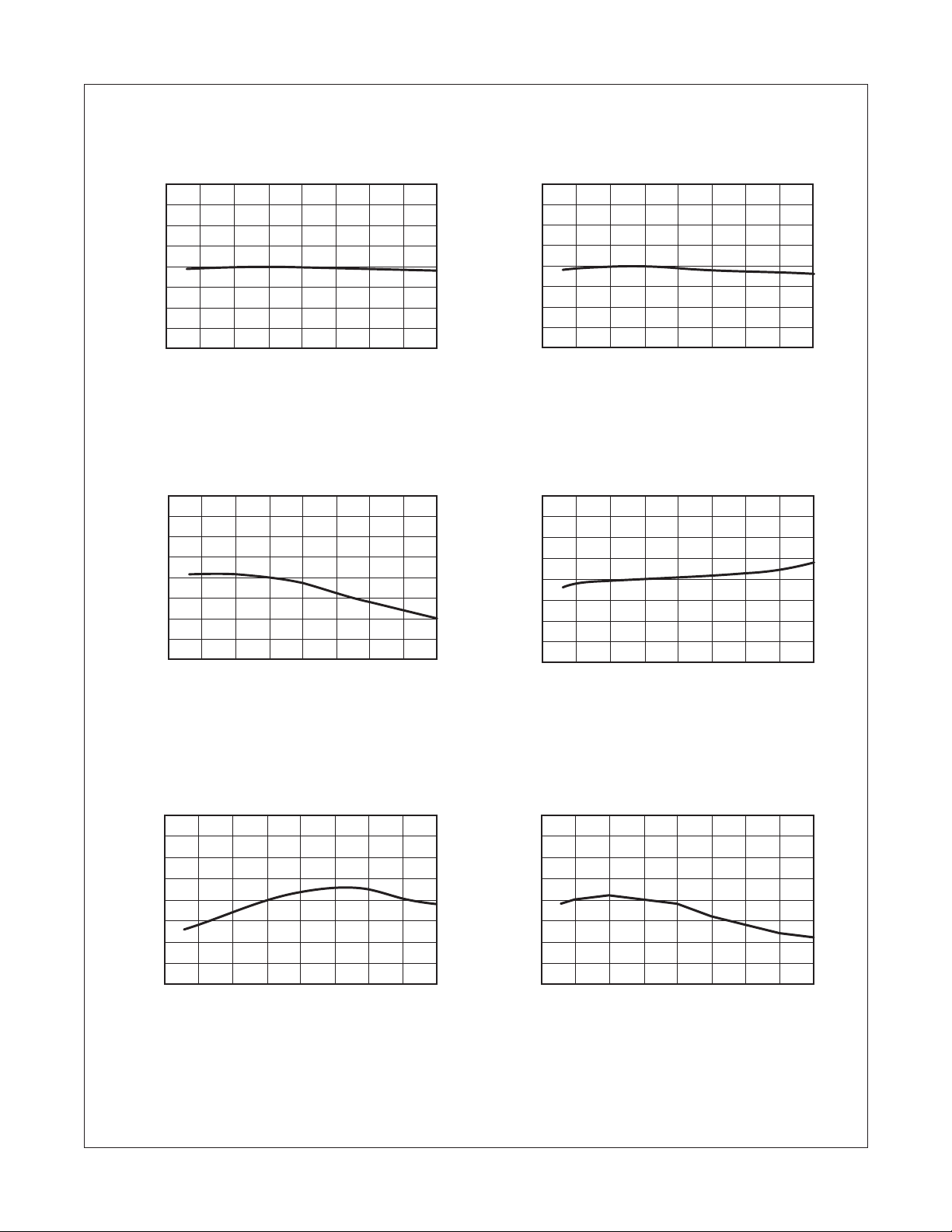
Electrical Characteristics (Continued)
Maximum Duty Cycle Over Voltage Protection
1.10
FSCQ-Series Green Mode Fairchild Power Switch (FPS™)
1.10
1.05
1.00
0.95
Normalized to 25°C
0.90
-50 0 50 100 150
Temp (°C)
Shutdown Delay Current Shutdown Feedback Voltage
1.2
1.1
1.0
0.9
Normalized to 25°C
0.8
-50 0 50 100 150
Temp (°C)
1.05
1.00
0.95
Normalized to 25°C
0.90
-50 0 50 100 150
Temp (°C)
1.10
1.05
1.00
0.95
Normalized to 25°C
0.90
-50 0 50 100 150
Temp (°C)
Feedback Source Current Burst Mode Feedback Source Current
1.2
1.1
1.0
0.9
Normalized to 25°C
0.8
-50 0 50 100 150
FSCQ-Series Rev. 1.1.2
Temp (°C)
1.2
1.1
11 www.fairchildsemi.com
1.0
0.9
Normalized to 25°C
0.8
-50 0 50 100 150
Temp (°C)
Electrical Characteristics (Continued)
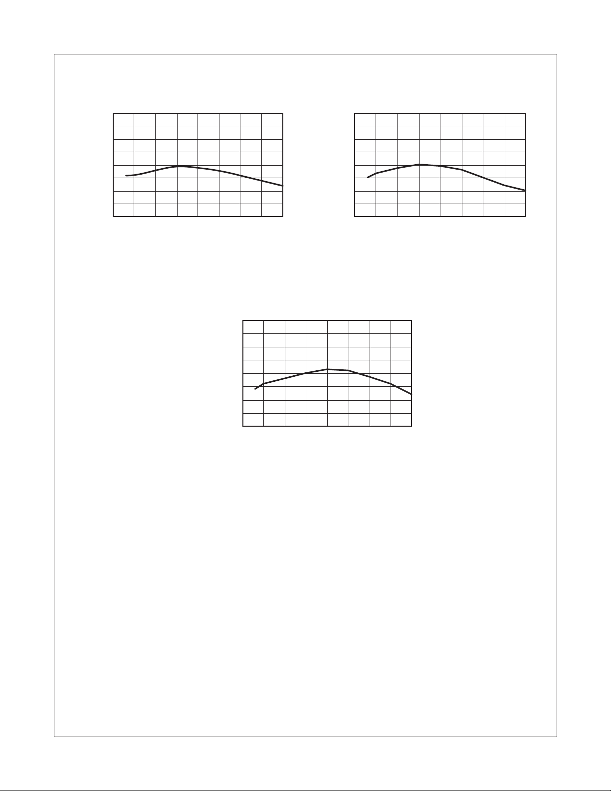
Feedback Offset Voltage Burst Mode Enable Feedback Voltage
1.4
FSCQ-Series Green Mode Fairchild Power Switch (FPS™)
1.4
1.2
1.0
0.8
Normalized to 25°C
0.6
-50 0 50 100 150
Temp (°C)
Sync. Threshold in Normal QR(H) Sync. Threshold in Normal QR(L)
1.10
1.05
1.00
0.95
Normalized to 25°C
0.90
-50 0 50 100 150
Temp (°C)
1.2
1.0
0.8
Normalized to 25°C
0.6
-50 0 50 100 150
Temp (°C)
1.10
1.05
1.00
0.95
Normalized to 25°C
0.90
-50 0 50 100 150
Temp (°C)
Sync. Threshold in Extended QR(H) Sync. Threshold in Extended QR(L)
1.10
1.05
1.00
0.95
Normalized to 25°C
0.90
-50 0 50 100 150
FSCQ-Series Rev. 1.1.2
Temp (°C)
1.10
1.05
1.00
0.95
Normalized to 25°C
0.90
-50 0 50 100 150
Temp (°C)
12 www.fairchildsemi.com
Electrical Characteristics (Continued)
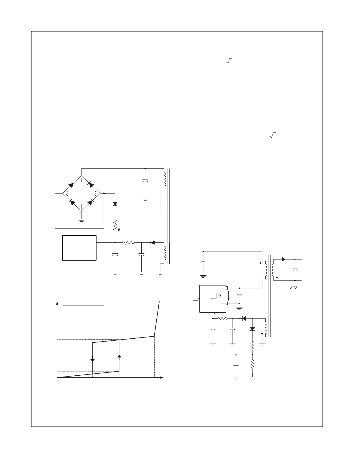
Extended QR Enable Frequency Extended QR Disable Frequency
1.10
FSCQ-Series Green Mode Fairchild Power Switch (FPS™)
1.10
1.05
1.00
0.95
Normalized to 25°C
0.90
-50 0 50 100 150
Temp (°C)
1.10
1.05
1.00
0.95
Normalized to 25°C
0.90
-50 0 50 100 150
1.05
1.00
0.95
Normalized to 25°C
0.90
-50 0 50 100 150
Temp (°C)
Pulse-by-pulse Current Limit
Temp (°C)
FSCQ-Series Rev. 1.1.2
13 www.fairchildsemi.com
FSCQ-Series Green Mode Fairchild Power Switch (FPS™)
Functional Description
1. Startup: Figure 4 shows the typical startup circuit and
the transformer auxiliary winding for the FSCQ-Series.
Before the FSCQ-Series begins switching, it consumes
only startup current (typically 25µA). The current supplied from the AC line charges the external capacitor
(C
) that is connected to the Vcc pin. When Vcc
a1
reaches the start voltage of 15V (V
Series begins switching, and its current consumption
increases to I
. Then, the FSCQ-Series continues its
OP
normal switching operation and the power required for
the FSCQ-Series is supplied from the transformer auxiliary winding, unless V
9V (V
control IC, V
). To guarantee the stable operation of the
STOP
has under voltage lockout (UVLO) with
CC
drops below the stop voltage of
CC
6V hysteresis. Figure 5 shows the relationship between
the operating supply current of the FSCQ-Series and the
supply voltage (V
AC line
min
(V
ac
– V
max
ac
).
CC
1N4007
I
)
sup
Rstr
V
CC
), the FSCQ-
START
C
DC
Da
The minimum average of the current supplied from the
AC is given by:
min
ac
V
--------------–
start
2
1
----------
•=
R
str
start
is the startup
str
is the
2V
⋅
where V
I
ac
avg
sup
min
---------------------------- -
π
is the minimum input voltage, V
FSCQ-Series start voltage (15V), and R
resistor. The startup resistor should be chosen so that
avg
I
is larger than the maximum startup current
sup
(50µA).
Once the resistor value is determined, the maximum loss
in the startup resistor is obtained as:
Loss
where V
max
V
()2V
ac
1
----------
R
str
max
ac
---------------------------------------------- -
•=
2
is the maximum input voltage. The star tup
2
start
22V
• V
---------------------------------------------------- -–
start
+
max
•
ac
π
resistor should have properly-rated dissipation wattage.
2. Synchronization: The FSCQ-Series employs a quasiresonant switching technique to minimize the switching
noise and loss. In this technique, a capacitor (Cr) is
added between the MOSFET drain and the source as
shown in Figure 6. The basic waveforms of the quasiresonant converter are shown in Figure 7. The external
capacitor lowers the rising slope of the drain voltage to
reduce the EMI caused when the MOSFET turns off. To
minimize the MOSFET’s switching loss, the MOSFET
should be turned on when the drain voltage reaches its
minimum value as shown in Figure 7.
FSCQ-Series
C
a1
C
Figure 4. Startup circuit
IOP Value
I
CC
FSCQ0565RT : 4mA (Typ.)
FSCQ0765RT : 4mA (Typ.)
FSCQ0965RT : 6mA (Typ.)
FSCQ1265RT : 6mA (Typ.)
FSCQ1465RT : 7mA (Typ.)
FSCQ1565RT : 7mA (Typ.)
FSCQ1565RP : 7mA (Typ.)
I
OP
Power Up
I
START
Power Down
Vstop = 9V VzVstart = 15V
Figure 5. Relationship Between Operating
Supply Current and Vcc Voltage
a2
C
DC
+
V
DC
–
Np
Lm
Ns
Vo
Drain
+
Cr
Ids
V
Sync
ds
–
GND
D
CO
a
Na
D
SY
R
SY1
R
SY2
V
CC
C
a1
V
CC
V
R
CC
C
a2
C
SY
Figure 6. Synchronization Circuit
FSCQ-Series Rev. 1.1.2
14 www.fairchildsemi.com
 Loading...