

Fairchild FSAV450 service manual
FSAV450
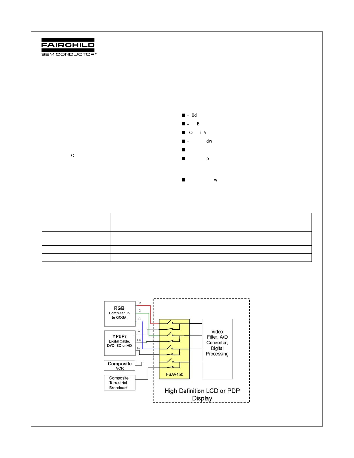
800MHz 4 Channel 2:1 Video Switch
FSAV450 800MHz 4 Channel 2:1 Video Switch
December 2004
Revised August 2005
General Description
The FSAV450 is a high performance Quad SPDT (2-to-1 multiplexer/demultiplexer) video switch designed specifically for
switching high definition YPbPr and computer RGB (up to
UXGA) signals. The bandwidth of this device is 800MHz (Typ)
which allows signals to pass with minimal edge and phase distortion. Image integrity is maintained with low crosstalk, high
OFF-Isolation and low differential gain and phase. The low On
:
Resistance (4
voltage operation (3V), low power consumption (1uA maximum)
and small scale packaging (including leadless DQFN) make this
device ideal for a broad range of applications.
typical) minimizes signal insertion loss. Low
Features
O
50dB OFF Isolation at 30MHz
O
80dB non-adjacent channel crosstalk at 30MHz
O4:
typical On Resistance (RON)
O
3dB bandwidth: 800MHz
O
Low power consumption (1uA max)
O
Control input: TTL compatible
Applications
O
RGB Video Switch in LCD, plasma and projector displays
Ordering Code:
Order Package
Number Number
FSAV450BQX
(Note 1)
FSAV450QSC MQA16A 16-Lead Quarter Size Outline Package (QSOP), JEDEC MO-137, 0.150 Wide
FSAV450MTC MTC16 16-Lead Thin Shrink Small Outline Package (TSSOP), JEDEC MO-153, 4.4mm Wide
Devices also available in Tape and Reel. Specify by appending suffix letter “X” to the ordering code.
Pb-Free package per JEDEC J-STD-020B.
Note 1: DQFN package available in Tape and Reel only.
MLP016E Pb-Free 16-T erminal Depopulat ed Quad Very-Thin Flat Pack No Leads (DQFN), JEDEC MO-241,
2.5 x 3.5mm
Package Description
© 2005 Fairchild Semiconductor Corporation DS500896 www.fairchildsemi.com
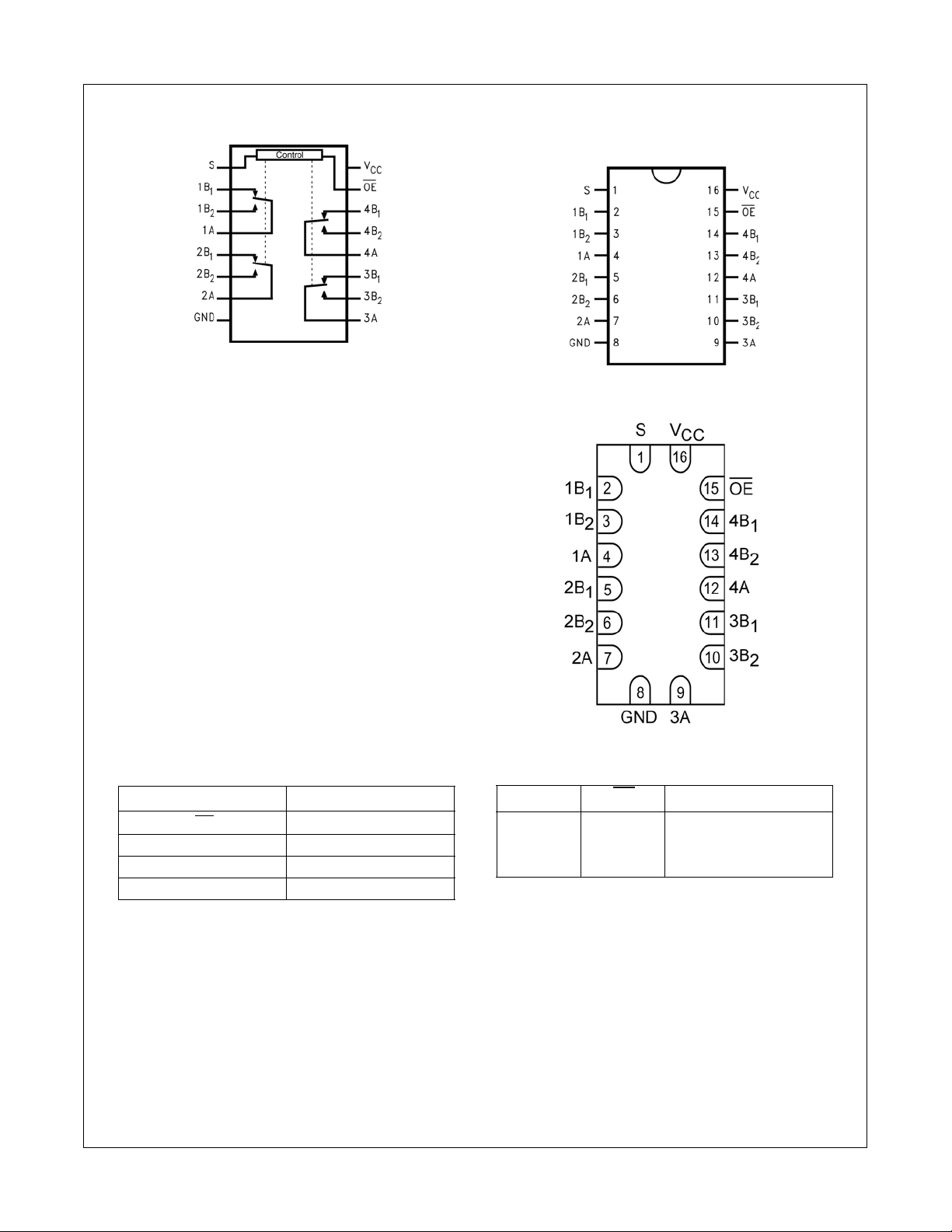
Analog Symbol
Connection Diagrams
FSAV450
Pin Assignments for QSOP and TSSOP
Pad Assignments for DQFN (Preliminary)
Pin Descriptions
Pin Name Description
OE Bus Switch Enable
S Select Input
ABus A
B
1–B2
www.fairchildsemi.com 2
Bus B
Truth Table
SOE Function
X H Disco nnect
LL A = B
HL A = B
1
2
FSAV450
Absolute Maximum Ratings(Note 2)
Supply Voltage (VCC)
DC Switch Voltage (V
DC Input Voltage (V
DC Input Diode Current (l
DC Output (I
DC V
OUT
/GND Current (ICC/I
CC
Storage Temperature Range (T
)
S
) (Note 3)
IN
) VIN 0V
IK
) Sink Current 128 mA
)
GND
)
STG
ESD
Human Body Model 2kV
0.5V to 6.0V
0.5V to 6.0V
0.5V to 6.0V
65q
C to 150 qC
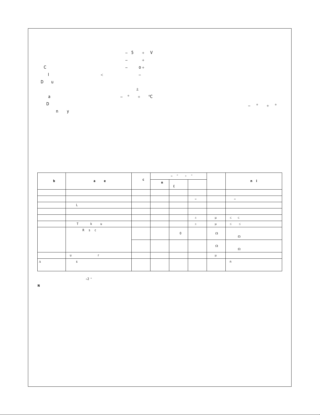
DC Electrical Characteristics
Symbol Parameter
Analog Signal Range 0 2.0 V
V
IK
V
IH
V
IL
I
I
I
OFF
R
ON
I
CC
'
I
CC
Clamp Diode Voltage 4.5
HIGH Level Input Voltage 4.5 to 5.5 2.0 V
LOW Level Input Voltage 4.5 to 5.5 0.8 V
Input Leakage Current 5.5
OFF-STATE Leakage Current 5.5
Switch On Resistance
(Note 6) RI = 75 :, ION = 13 mA
Quiescent Supply Current 5.5 1.0
Increase in I
per Input 5.5 1.5 mA One Input at 3.4V
CC
Recommended Operating Conditions
(Note 4)
Power Supply Operating (VCC) 4.5V to 5.5V
Input Voltage (V
50 mA
r
100 mA
V
CC
(V)
4.5 4.0 6.0
4.5 5.0 7.0
Output Voltage (V
Input Rise and Fall Time (tr, tf)
Switch Control Input 0 ns/V to 5 ns/V
Switch I/O 0 ns/V to DC
Free Air Operating Temperature (T
Note 2: The Absolute Maximum Ratings are those values beyond which the safety of
the device cannot be guaranteed. The device should not be operated at these limits.
The parametric values defined in the Electrical Characteristics tables are not guaranteed at the absolute maximum rating. The Recommended Operating Conditions
tables will define the conditions for actual device operation.
Note 3: The input and output negative voltage ratings may be exceeded if the input
and output diode current ratings are observed.
Note 4: Unused control inputs must be held HIGH or LOW. They may not float.
TA = 40 qC to 85 qC
Min Typ
(Note 5)
)0V to V
IN
)0V to V
OUT
)
A
Max
1.2 V IIN = 18 mA
r
1.0
r
1.0
Units Conditions
P
A0 d VIN d 5.5V
P
A0 d A, B d V
VIN = 1.0V
:
VIN = 2.0V
:
RI = 75 :, ION = 26 mA
P
AVIN = VCC or GND, I
Other Inputs at VCC or GND
40 qC to 85 qC
CC
OUT
CC
CC
= 0
Note 5: Typical values are at TA = 25qC
Note 6: Measured by the voltage drop between A and B pins at the indicated current through the switch. On Resistance is determined by the lower of the voltages on the two
(A or B) pi ns.
3 www.fairchildsemi.com

AC Electrical Characteristics
T
FSAV450
Symbol Parameter
t
ON
t
OFF
DG Differential Gain 4.5 to 5.5 0.2 % RL = 75:, f= 3.58MHz Figure 2
DP Differential Phase 4.5 to 5.5 0.1 Degree RL = 75:, f= 3.58MHz Figure 3
O
IRR
X
TALK
BW
Note 7: Typical values are at VCC = 5.0V and TA = 25qC
Turn ON Time S-to-Bus B 4.5 to 5.5 4.0 6.0
Output Enable Time OE-to-A or B 4.5 to 5.5 3.5 5.5
Turn OFF Time S-to-Bus B 4.5 to 5.5 1.5 3.5
Output Disable Time OE-to-A or B 4.5 to 5.5 1.5 3.5
Non-Adjacent OFF-Isolation 4.5 to 5.5
Non-Adjacent Channel Crosstalk 4.5 to 5.5
3dB Bandwidth 4.5 to 5.5 800
V
CC
(V)
4.5 to 5.5 700 R
4.5 to 5.5 650 RL = 75: (DQFN)
4.5 to 5.5 600 RL = 75: (QSOP and TSSOP)
= 40qC to 85qC
A
Min Typ
(Note 7)
50.0
80.0
Max
Units Conditions
ns VB = 2.0V
ns VB = 2.0V
f = 30MHz, RL = 75
dB
RL = 75:, f= 30MHz Figures
dB
RL = 50: (DQFN) Figures
= 50: (QSOP and TSSOP)
L
MHz
:
Capacitance
Figure
Number
Figures
8, 9
Figures
8, 9
Figures
4, 10
5, 11
1, 12
Figure
12
Symbol Parameter
C
IN
C
ON
C
OFF
Control Pin Input Capacitance 3.0 pF VCC = 0V
A/B ON Capacitance 8.5 pF VCC = 5.0V, OE = 0V
Port B OFF Capacitance 3.0 pF VCC and OE = 5.0V
TA = 40qC to 85qC
Typ
FIGURE 1. Gain vs. Freq u e nc y
Units Conditions
www.fairchildsemi.com 4
 Loading...