

FDT3612
FDT3612
100V N-Channel PowerTrench
General Description
This N-Channel MOSFET has been designed
specifically to i mprove the overall efficiency of DC/DC
converters using either synchronous or conventional
switching PW M controllers.
These MOSFETs feature faster switching and lower
gate charge than other MOSFETs with comparable
R
specifications. The result is a MOSFET that is
DS(ON)
easy and safer to drive (even at very high frequenc ies),
and DC/DC power supply designs with higher overall
efficiency.
Applications
• DC/DC converter
• Motor driving
MOSFET
D
February 2012
Features
• 3.7 A, 100 V. R
R
• Fast switching speed
• Low gate charge (14nC typ)
• High performance trench technology for extremely
DS(ON)
low R
• High power and current handling capability in a
widely used surface mount pac kage
= 120 mΩ @ VGS = 10 V
DS(ON)
= 130 mΩ @ VGS = 6 V
DS(ON)
D
D
S
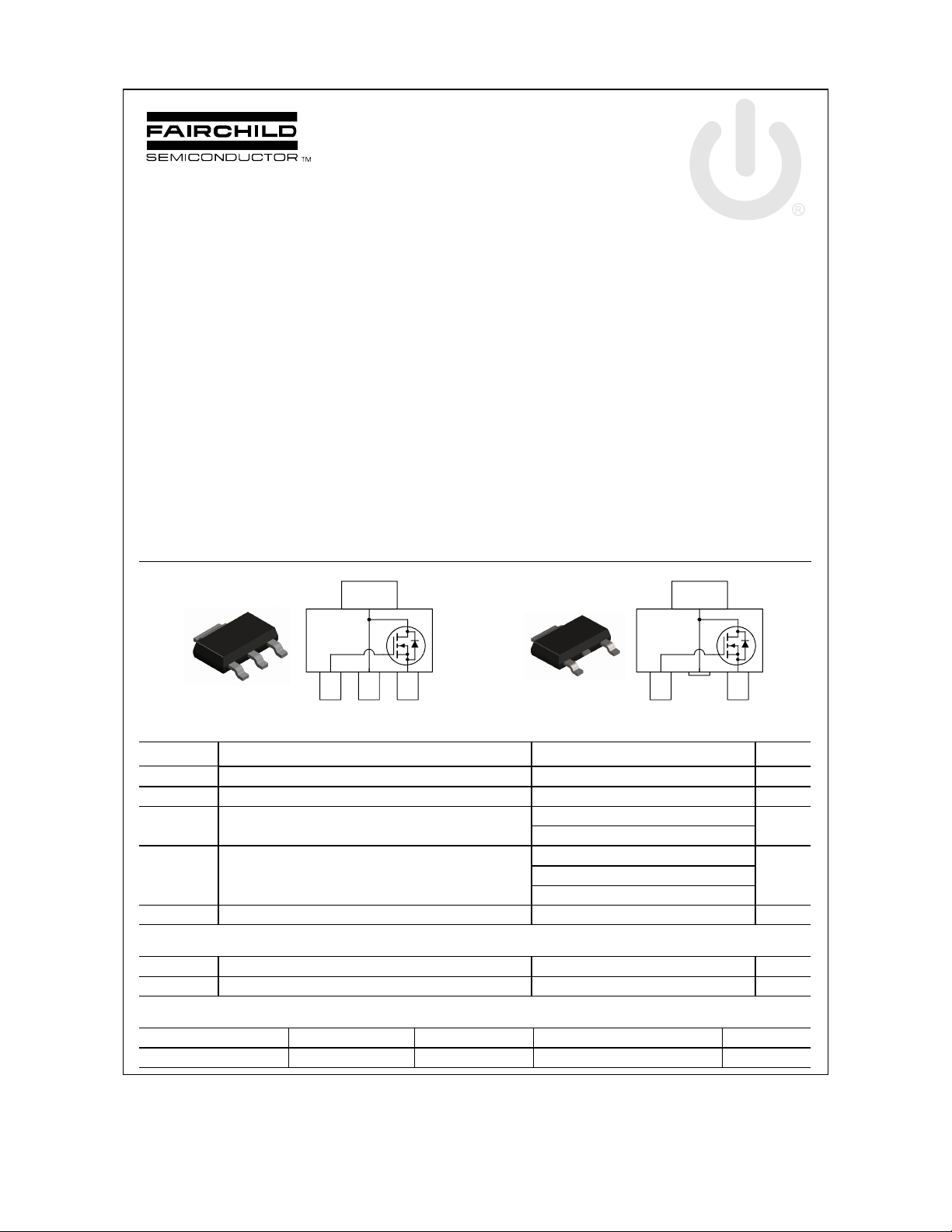
SOT-22 3
D
G
SG
D
Absolute Maximum Ratings T
o
=25
C unless otherwise noted
A
D
SOT-223
(J23Z)
S
G
*
G
S
Symbol Parameter Ratings Units
V
Drain-Source Voltage 100 V
DSS
V
Gate-Source Voltage
GSS
±20
V
ID Drain Current – Continuous (Note 1a) 3.7 A
– Pulsed 20
PD
Maximum Power Dissipation (Note 1a) 3.0
(Note 1b)
TJ, T
Operating and Storage Junction Temperature Range –55 to +150
STG
(Note 1c)
1.3
1.1
W
°C
Thermal Characteristics
R
θJA
R
θJC
Thermal Resistance, Junction-to-Ambient
Thermal Resistance, Junction-to-Case
(Note 1a) 42
(Note 1) 12
°C/W
°C/W
Package Marking and Ordering Information
Device Marking Device Reel Size Tape width Quantity
3612 FDT3612 13’’ 12mm 2500 units
2012 Fairchild Semiconductor Corporation
FDT3612 Rev. C2 (W)
FDT3612
Electrical Characteristics T
= 25°C unless otherwise noted
A
Symbol Parameter Test Conditions Min Typ Max Units
Drain-Source Avalanche Ratings (Note 2)
W
Drain-Source Avalanche Energy Single Pulse, VDD = 50 V, ID= 3.7 A 90 mJ
DSS
IAR Drain-Source Avalanche Current 3.7 A
Off Characteristics
BV
Drain–Source Breakdown Voltage
DSS
∆BVDSS
∆T
I
Zero Gate Voltage Drain Current VDS = 80 V, VGS = 0 V 10
DSS
I
GSSF
I
GSSR
Breakdown Voltage Temperature
Coefficient
J
Gate–Body Leakage, Forward VGS = 20 V, VDS = 0 V 100 nA
Gate–Body Leakage, Reverse VGS = –20 V, VDS = 0 V –100 nA
= 0 V, ID = 250 µA
V
GS
I
= 250 µA, Referenced to 25°C
D
100 V
106
mV/°C
µA
On Characteristics (Note 2)
V
Gate Threshold Voltage
GS(th)
∆VGS(th)
∆TJ
R
DS(on)
Gate Threshold Voltage
Temperature Coefficient
Static Drain–Source
On–Resistance
I
On–State Drain Current VGS = 10 V, VDS = 10 V 10 A
D(on)
= VGS, ID = 250 µA
V
DS
= 250 µA, Referenced to 25°C
I
D
VGS = 10 V, ID = 3.7 A
= 6 V, ID = 3.5 A
V
GS
V
= 10 V, ID = 3.7A, TJ = 125°C
GS
gFS Forward Transconductance VDS = 10 V, ID = 3.7 A 11 S
2 2.5 4 V
–6
88
94
170
120
130
245
mV/°C
mΩ
Dynamic Characteristics
C
Input Capacitance 632 pF
iss
C
Output Capacitance 40 pF
oss
C
Reverse Transfer Capacitance
rss
= 50 V, V
V
DS
f = 1.0 MHz
= 0 V,
GS
20 pF
Switching Characteristics (Note 2)
t
Turn–On Delay Time 8.5 17 ns
d(on)
tr Turn–On Rise Time 2 4 ns
t
Turn–Off Delay Time 23 37 ns
d(off)
tf Turn–Off Fall Time
Qg Total Gate Charge 14 20 nC
Qgs Gate–Source Charge 2.4 nC
Qgd Gate–Drain Charge
V
= 50 V, ID = 1 A,
DD
= 10 V, R
V
GS
V
= 50 V, ID = 3.7 A,
DS
V
= 10 V
GS
GEN
= 6 Ω
4.5 9 ns
3.8 nC
Drain–Source Diode Characteristics and Maximum Ratings
IS Maximum Continuous Drain–Source Di ode Forward Current 2.5 A
VSD Drain–Source Diode Forward
Voltage
Notes:
1. R
is the sum of the junction-to-case and case-to-ambient thermal resistance where the case thermal reference is defined as the solder mounting surface of
θJA
the drain pins. R
2. Pulse Test: Pulse Width < 300µs, Duty Cycle < 2.0%
is guaranteed by design while R
θJC
a) 42°C/W when
mounted on a 1in
pad of 2 oz copper
is determined by the user's board design.
θCA
2
VGS = 0 V, IS = 2.5 A (Note 2)
b) 95°C/W when
mounted on a .0066
2
pad of 2 oz
in
copper
0.75 1.2 V
c) 110°C/W when mounted on a
minimum pad.
FDT3612 Rev. C2 (W)

Typical Characteristics
FDT3612
20
VGS = 10V
16
12
8
, DRAIN CURRENT (A)
D
I
4
0
02468
5.0V
V
, DRAIN-SOURCE VOLTAGE (V)
DS
4.5V
4.0V
3.5V
1.8
1.6
VGS = 4.0V
4.5V
5.0V
6.0V
10V
1
0 4 8 12 16 20
, DRAIN CURRENT (A)
I
D
, NORMALIZED
DS(ON)
R
1.4
1.2
DRAIN-SOURCE ON-RESISTANCE
0.8
Figure 1. On-Region Characteristics. Figure 2. On-Resistance Variation with
Drain Current and Gate Voltage.
2.2
ID = 3.7A
2
V
= 10V
GS
1.8
1.6
1.4
1.2
, NORMALIZED
1
DS(ON)
R
0.8
0.6
DRAIN-SOURCE ON-RESISTANCE
0.4
-50 -25 0 25 50 75 100 125 150
T
, JUNCTION TEMPERATURE (oC)
J
0.4
0.3
0.2
, ON-RESISTANCE (OHM)
0.1
DS(ON)
R
0
345678910
, GATE TO SOURCE VOLTAGE (V)
V
GS
TA = 125oC
TA = 25oC
ID = 1.9 A
Figure 3. On-Resistance Variation with
Temperature.
20
VDS = 10V
16
12
8
, DRAIN CURRENT (A)
D
I
4
0
22.533.544.55
TA = 125oC
-55oC
V
, GATE TO SOURCE VOLTAGE (V)
GS
25oC
Figure 5. Transfer Characteristics. Figure 6. Body Diode Forward Voltage Variation
Figure 4. On-Resistance Variation with
Gate-to-Source Voltage.
100
VGS = 0V
10
1
0.1
0.01
0.001
, REVERSE DRAIN CURRENT (A)
S
I
0.0001
0 0.2 0.4 0.6 0.8 1 1.2 1.4
TA = 125oC
25oC
-55oC
, BODY DIODE FORWARD VOLTAGE (V)
V
SD
with Source Current and Temperature.
FDT3612 Rev. C2 (W)

Typical Characteristics
FDT3612
10
ID = 3.7A
8
6
4
2
, GATE-SOURCE VOLTAGE (V)
GS
V
0
0 2 4 6 8 10 12 14 16
Q
, GATE CHARGE (nC)
g
VDS = 40V
80V
60V
800
700
600
500
400
300
CAPACITANCE (pF)
200
100
0
C
RSS
0 20406080100
V
, DRAIN TO SOURCE VOLT AGE ( V )
DS
C
ISS
C
OSS
Figure 7. Gate Charge Characteristics. Figure 8. Capacitance Characteristics.
50
10
1
THIS A REA IS
0.1
LIMITED BY r
SINGLE PULSE
, DRAIN CURRENT (A)
D
I
0.01
0.001
= MAX RATED
T
J
R
θJA
= 25
T
A
0.1 1 10 100 500
DS(on)
o
= 110
C/W
o
C
VDS, DRAIN to SOURCE VOLTAGE (V)
100 μs
1 ms
10 ms
100 ms
1 s
10 s
DC
40
SINGLE PULSE
R
30
20
10
P(pk), PEAK TRANSIENT POWER (W)
0
0.001 0.01 0.1 1 10 100
, TIME (sec)
t
1
θ
Figure 9. Maximum Safe Operating Area. Figure 10. Single Pulse Maximum
Power Dissipation.
= 110°C/W
JA
T
= 25°C
A
f = 1MHz
= 0 V
V
GS
1
D = 0.5
0.2
0.1
0.01
r(t), NORMALIZED EFFECTIVE
0.001
TRANSIENT THERMAL RESISTANCE
0.0001 0.001 0.01 0.1 1 10 100 1000
0.1
0.05
0.02
0.01
SINGLE PULSE
, TIME (sec)
t
1
Figure 11. Transient Thermal Response Curve.
Thermal characterization performed using the conditions described in Note 1c.
Transient thermal response will change depending on the circuit board design.
R
(t) = r(t) + R
θJA
R
= 110°C/W
JA
θ
)
P(pk
t
1
t
T
- TA = P * R
J
Duty Cycle, D = t
θJA
2
(t)
θJA
/ t
1
2
FDT3612 Rev. C2 (W)

TRADEMARKS
®
™
tm
tm
The following includes registered and unregistered trademarks and service marks, owned by Fairchild S emiconductor and/or its global su bsidiaries, and is not
intended to be an exhaustive list of all such trademarks.
2Cool™
AccuPower™
AX-CAP™*
®
BitSiC
Build it Now™
CorePLUS™
CorePOWER™
CROSSVOLT™
CTL™
Current Transfer Logic™
DEUXPEED
Dual Cool™
EcoSPARK
EfficentMax™
ESBC™
Fairchild
Fairchild Semiconductor
FACT Quiet Series™
FACT
FAST
FastvCore™
FETBench™
FlashWriter
FPS™
®
®
®
®
®
®
*
®
F-PFS™
®
FRFET
Global Power Resource
Green Bridge™
Green FPS™
Green FPS™ e-Series™
Gmax™
GTO™
IntelliMAX™
ISOPLANAR™
Marking Small Speakers Sound Louder
and Better™
MegaBuck™
MICROCOUPLER™
MicroFET™
MicroPak™
MicroPak2™
MillerDrive™
MotionMax™
Motion-SPM™
mWSaver™
OptoHiT™
OPTOLOGIC
OPTOPLANAR
®
®
®
PowerTrench
SM
PowerXS™
Programmable Active Droop™
QFET
QS™
Quiet Series™
RapidConfigure™
Saving our world, 1mW/W/kW at a time™
SignalWise™
SmartMax™
SMART START™
Solutions for Your Success™
SPM
STEALTH™
SuperFET
SuperSOT™-3
SuperSOT™-6
SuperSOT™-8
SupreMOS
SyncFET™
Sync-Lock™
®
®
®
®
®
®*
The Power Franchise
TinyBoost™
TinyBuck™
TinyCalc™
®
TinyLogic
TINYOPTO™
TinyPower™
TinyPWM™
TinyWire™
®
TranSiC
TriFault Detect™
TRUECURRENT
μSerDes™
®
UHC
Ultra FRFET™
UniFET™
VCX™
VisualMax™
VoltagePlus™
XS™
®
®
®
*
*Trademarks of System General Corporation, used under license by Fairchild Semiconductor.
DISCLAIMER
FAIRCHILD SEMICONDUCTOR RESERVES THE RIGHT TO MAKE CHANGES WITHOUT FURTHER NOTICE TO ANY PRODUCTS HEREIN TO IMPROVE
RELIABILITY, FUNCTION, OR DESIGN. FAIRCHILD DOES NOT ASSUME ANY LIABILITY ARISING OUT OF THE APPLICATION OR USE OF ANY
PRODUCT OR CIRCUIT DESCRIBED HEREIN; NEITHER DOES IT CONVEY ANY LICENSE UNDER ITS PATENT RIGHTS, NOR THE RIGHTS OF OTHERS.
THESE SPECIFICATIONS DO NOT EXPAND THE TERMS OF FAIRCHILD’S WORLDWIDE TERMS AND CONDITIONS, SPECIFICALLY THE WARRANTY
THEREIN, WHICH COVERS THESE PRODUCTS.
LIFE SUPPORT POLICY
FAIRCHILD’S PRODUCTS ARE NOT AUTHORIZED FOR USE AS CRITICAL COMPONENTS IN LIFE SUPPORT DEVICES OR SYSTEMS WITHOUT THE
EXPRESS WRITTEN APPROVAL OF FAIRCHILD SEMICONDUCTOR CORPORATION.
As used here in:
1. Life support devices or systems are devices or systems which, (a) are
intended for surgical implant into the body or (b) sup port or su stain li fe,
and (c) whose failure to perform when properly used in accordance with
instructions for use provided in the labeling, can be reasonably
expected to result in a significant injury of the user.
ANTI-COUNTERFEITING POLICY
Fairchild Semiconductor Corporation’s Anti-Counterfeiting Policy. Fairchild’s Anti-Counterfeiting Policy is also stated on our external website,
www.Fairchildsemi.com, under Sales Support
Counterfeiting of semiconductor parts is a growing problem in the industry. Al l manufactures of semicond uctor products are experiencing counterf eiting of their
parts. Customers who inadvertently purchase counterfeit parts ex perience many problems such as loss of brand reputa tion, substa ndard pe rformance, f ail ed
application, and increased cost of production and manufacturing delays. Fairchild is taking st ron g measures to prote ct ourselve s and our customers from the
proliferation of counterfeit parts. Fairchild strongly encourages customers to purchase Fairchild pa rts either direct ly from Fairchild or from Authori zed Fairchild
Distributors who are listed by country on our web page cited above. Products customers buy either from Fairchild directly or from Authorized Fairchild
Distributors are genuine parts, have full traceability, meet Fa irchild’s quality standards for handing and storage and provide access to Fairchild’s full range of
up-to-date technical and product information. Fairchild and our Authorized Distributors will stand behind all warranties and will appropriately address and
warranty issues that may arise. Fairchild will not provide any warranty coverage or other assistance for parts bought from Unauthorized Sources. Fairchild is
committed to combat this global problem and encourage our customers to do their part in stopping this practice by buying direct or from authorized dist ributors.
.
2. A critical component in any component of a life support, device, or
system whose failure to perform can be reasonably expected to cause
the failure of the life support device or system, or to affect its safety or
effectiveness.
PRODUCT STATUS DEFINITIONS
Definition of Terms
Datasheet Identification Product Status Definition
Advance Information Formative / In Design
Preliminary First Production
No Identification Needed Full Production
Obsolete Not In Production
Datasheet contains the design specifications for product development. Specifications
may change in any manner without notice.
Datasheet contains preliminary data; supplementary data will be published at a later
date. Fairchild Semiconductor reserves the right to make changes at any time without
notice to improve design.
Datasheet contains final specifications. Fairchild Semiconductor rese rves the right to
make changes at any time without notice to improve the design.
Datasheet contains specifications on a product that is discontinued by Fairchild
Semiconductor. The datasheet is for reference information only.
Rev. I61
 Loading...