

tm
FDS9958
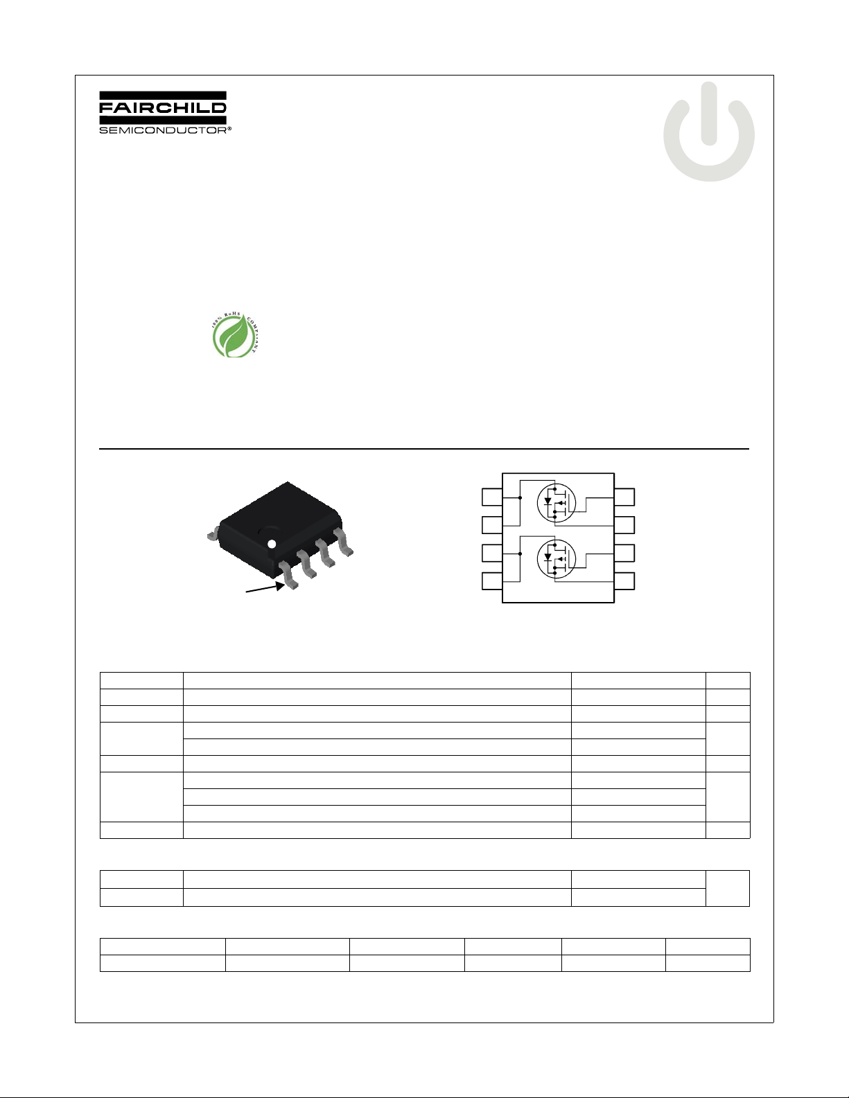
Dual P-Channel PowerTrench® MOSFET
-60V, -2.9A, 105mΩ
Features
Max r
Max r
RoHS Compliant
=105mΩ at VGS = -10V, ID = -2.9A
DS(on)
=135mΩ at VGS = -4.5V, ID = -2.5A
DS(on)
D2
D2
D1
D1
General Description
These P-channel logic level specified MOSFETs are produced
using Fairchild Semiconductor’s advanced PowerTrench
process that has been especially tailored to minimize the
on-state resistance and yet maintain low gate charge for superior
switching performance.
These devices are well suited for portable electronics
applications: load switching and power management, battery
charging and protection circuits.
Applications
Load Switch
Power Management
D2
5
D2
6
Q2Q1Q2
FDS9958 Dual P-Channel PowerTrench
July 2007
®
®
MOSFET
G2
4
S2
3
G2
S2
G1
SO-8
S1
= 25°C unless otherwise noted
A
Pin 1
MOSFET Maximum Ratings T
Symbol Parameter Ratings Units
V
DS
V
GS
I
D
E
AS
P
D
, T
T
J
STG
Drain to Source Voltage -60 V
Gate to Source Voltage ±20 V
Drain Current -Continuous (Note 1a) -2.9
-Pulsed -12
Single Pulse Avalanche Energy (Note 3) 54 mJ
Power Dissipation for Dual Operation 2
Power Dissipation (Note 1b) 0.9
Operating and Storage Junction Temperature Range -55 to +150 °C
D1
D1
7
Q1
8
G1
2
S1
1
Thermal Characteristics
R
θJC
R
θJA
Thermal Resistance, Junction to Case 40
Thermal Resistance, Junction to Ambient (Note 1a) 78
Package Marking and Ordering Information
Device Marking Device Package Reel Size Tape Width Quantity
FDS9958 FDS9958 SO-8 330mm 12mm 2500units
A
WPower Dissipation (Note 1a) 1.6
°C/W
©2007 Fairchild Semiconductor Corporation
FDS9958 Rev.C
1
www.fairchildsemi.com
FDS9958 Dual P-Channel PowerTrench
Electrical Characteristics T
= 25°C unless otherwise noted
J
Symbol Parameter Test Conditions Min Typ Max Units
Off Characteristics
BV
DSS
∆BV
DSS
∆T
J
I
DSS
I
GSS
On Characteristics
V
GS(th)
∆V
GS(th)
∆T
J
r
DS(on)
g
FS
Drain to Source Breakdown Voltage ID = -250µA, VGS = 0V -60 V
Breakdown Voltage Temperature
Coefficient
Zero Gate Voltage Drain Current
Gate to Source Leakage Current VGS = ±20V, V
ID = -250µA, referenced to 25°C -52 mV/°C
VDS = -48V, -1
V
= 0V TJ = 125°C -100
GS
= 0V ±100 nA
DS
Gate to Source Threshold Voltage VGS = VDS, ID = -250µA -1.0 -1.6 -3.0 V
Gate to Source Threshold Voltage
Temperature Coefficient
Static Drain to Source On Resistance
Forward Transconductance VDD = -5V, ID = -2.9A 7.7 S
ID = -250µA, referenced to 25°C 4 mV/°C
VGS = -10V, ID = -2.9A 82 105
VGS = -10V, ID = -2.9A, TJ= 125°C 131 190
Dynamic Characteristics
C
iss
C
oss
C
rss
Input Capacitance
Output Capacitance 90 120 pF
Reverse Transfer Capacitance 40 65 pF
VDS = -30V, VGS = 0V,
f = 1MHz
765 1020 pF
Switching Characteristics
t
d(on)
t
r
t
d(off)
t
f
Q
Q
Q
Q
g
g
gs
gd
Turn-On Delay Time
Rise Time 3 10 ns
Turn-Off Delay Time 27 43 ns
VDD = -30V, ID = -2.9A,
VGS = -10V, R
GEN
= 6Ω
6 12 ns
Fall Time 6 12 ns
Total Gate Charge V
Total Gate Charge V
Gate to Source Charge 2 nC
= 0V to -10V
GS
= 0V to -4.5V 8 12 nC
GS
VDD = -30V,
ID = -2.9A
16 23 nC
Gate to Drain “Miller” Charge 3 nC
µA
mΩVGS = -4.5V, ID = -2.5A 103 135
®
MOSFET
Drain-Source Diode Characteristics
V
SD
t
rr
Q
rr
NOTES:
1. R
is determined with the device mounted on a 1in2 pad 2 oz copper pad on a 1.5 x 1.5 in. board of FR-4 material. R
θJA
the user's board design.
2. Pulse Test: Pulse Width < 300µs, Duty cycle < 2.0%.
3. UIL condition: Starting T
©2007 Fairchild Semiconductor Corporation
FDS9958 Rev.C
Source to Drain Diode Forward Voltage V
Reverse Recovery Time
Reverse Recovery Charge 21 35 nC
= 25°C, L = 3mH, I
J
a) 78°C/W when
mounted on a 1 in
pad of 2 oz copper
= 6A, VDD = 60V, VGS = 10V.
AS
= 0V, IS = -1.3A (Note 2) -0.8 -1.2 V
GS
IF = -2.9A, di/dt = 100A/µs
2
2
θJC
26 42 ns
is guaranteed by design while R
b) 135°C/W when
mounted on a
minimun pad
is determined by
θCA
www.fairchildsemi.com

FDS9958 Dual P-Channel PowerTrench
Typical Characteristics T
12
VGS = -10V
10
8
6
4
, DRAIN CURRENT (A)
D
2
-I
0
01234
-V
DS
Figure 1.
On-Region Characteristics
1.8
ID = -2.9A
V
GS
= -10V
1.6
1.4
1.2
NORMALIZED
1.0
0.8
DRAIN TO SOURCE ON-RESISTANCE
0.6
-75 -50 -25 0 25 50 75 100 125 150
T
, JUNCTION TEMPERATURE (
J
Figu r e 3. Nor m a lized O n - Resis t a nce
vs Junction Temperature
VGS = - 4V
VGS = -5V
VGS = - 4.5V
PULSE DURA TION = 300µs
DUTY CYCLE = 2.0%MAX
, DRAIN TO SOURCE VOLTAGE (V)
= 25°C unless otherwise noted
J
VGS = -3.5V
VGS = -3V
o
C)
2.5
VGS = -3V
2.0
1.5
NORMALIZED
1.0
PULSE DURATION = 300µs
DRAIN TO SOURCE ON-RESISTANCE
0.5
Figure 2.
DUTY CYCLE = 2.0%MAX
024681012
-I
D
Norma l i z e d O n - Resistanc e
VGS = -3.5V
VGS = -4.5V
, DRAIN CURRENT(A)
VGS = -4V
V
= -5V
GS
V
= -10V
GS
vs Drain Current and Gate Voltage
240
210
ID = -2.9A
(mΩ)
180
150
, DRAIN TO
120
DS(on)
r
90
SOURCE ON-RESISTANCE
60
246810
-V
, GATE TO SO U RCE VOLTAGE (V)
GS
Figure 4.
On-Resistance vs Gate to
PULSE DURA TION = 300µs
DUTY CYCLE = 2.0%MAX
TJ = 125oC
o
T
= 25
C
J
Source Voltage
®
MOSFET
12
PULSE DURATION = 300µs
DUTY CYCLE = 2.0%MAX
10
V
= -5V
DD
8
6
4
, DRAIN CURRENT (A)
D
2
-I
0
012345
TJ = 150oC
TJ = 25oC
-VGS, GATE TO SOURCE VOLTAGE (V)
Figure 5. Transfer Characteristics
©2007 Fairchild Semiconductor Corporation
FDS9958 Rev.C
TJ = -55oC
20
10
V
= 0V
GS
1
0.1
TJ = 150oC
TJ = 25oC
TJ = -55oC
0.01
, REVERSE DRAIN CURRENT (A)
S
-I
1E-3
0.0 0.2 0.4 0.6 0.8 1.0 1.2
-VSD, BODY DIODE FORWARD VOLTAGE (V)
Figure 6.
Source to Drain Diode
Forward Voltage vs Source Current
3
www.fairchildsemi.com

FDS9958 Dual P-Channel PowerTrench
Typical Characteristics T
10
ID = -2.9A
8
6
4
VDD = -30V
2
, GATE TO SOURCE VOLTAGE(V)
GS
-V
0
0 5 10 15 20
Figure 7.
4
3
2
, AVALANCHE CURRENT(A)
AS
-I
1
0.01 0.1 1 10 100
Figure 9.
Switching Capability
V
= -20V
DD
VDD = -40V
Qg, GATE CHARGE(nC)
Gate Charge Characteristics
TJ = 125oC
tAV, TIME IN AVALANCHE(ms )
Uncl a m p e d I n duct i v e
= 25°C unless otherwise noted
J
TJ = 25oC
2000
1000
C
iss
100
CAPACITANCE (pF)
f = 1MHz
V
= 0V
GS
10
0.1 1 10
-VDS, DRAIN TO SOURCE VOLTAGE (V)
Figure 8.
Capacitance vs Drain
C
oss
C
rss
to Source Voltage
3.0
2.5
2.0
V
GS
= -4.5V
V
1.5
1.0
, DRAIN CURRENT (A)
-I
R
D
θJA
= 78oC/W
0.5
0.0
25 50 75 100 125 150
T
, AMBIENT TEMPERATURE (
A
Figure 10.
Ma xim um Continuou s Dr ain
Current vs Ambient Temperature
60
®
MOSFET
= -10V
GS
o
C)
20
10
1
THIS A REA IS
LIMITED BY r
0.1
, DRAIN CURRENT (A)
D
-I
0.01
0.1 1 10 100
DS(on)
SINGLE PULSE
T
= MAX RATED
J
o
= 135
θJA
A
= 25
C/W
o
C
R
T
-VDS, DRAIN to SOURCE VOLTAGE (V)
Figure 11. Forward Bias Safe
Operating Area
©2007 Fairchild Semiconductor Corporation
FDS9958 Rev.C
200
0.1ms
1ms
10ms
100ms
1s
10s
DC
200
100
10
1
), PEAK TRANSIENT POWER (W)
PK
P(
0.5
Figure 12.
VGS = -10V
10-310-210
t, PULSE WIDTH (s)
Sing le Pulse Maxim um
SINGLE PULSE
o
R
= 135
C/W
θJA
o
T
= 25
C
A
-1
0
10
10110210
3
Power Dissipation
4
www.fairchildsemi.com

FDS9958 Dual P-Channel PowerTrench
Typical Characteristics T
NORMALIZED THERMAL
θJA
Z
0.1
IMPEDANCE,
0.01
0.005
2
1
DUTY CYCLE-DESCENDING ORDER
D = 0.5
0.2
0.1
0.05
0.02
0.01
-3
10
10
-2
= 25°C unless otherwise noted
J
SINGLE PULSE
= 135oC/W
R
θJA
10
-1
t, RECTANGULAR PULSE DURATION (s)
0
10
NOTES:
DUTY FACTOR: D = t
PEAK TJ = PDM x Z
1
10
Figure 13. Transient Thermal Response Curve
P
DM
t
1
t
2
1/t2
x R
+ T
θJA
θJA
A
2
10
3
10
®
MOSFET
©2007 Fairchild Semiconductor Corporation
FDS9958 Rev.C
5
www.fairchildsemi.com

TRADEMARKS
The following are registered and unregistered trademarks and service marks Fairchild Semiconductor owns or is authorized to use and
is not intended to be an exhaustive list of all such trademarks.
®
ACEx
Build it Now™
CorePLUS™
CROSSVOLT™
CTL™
Current Transfer Logic™
EcoSPARK
Fairchild
®
®
Fairchild Semiconductor
FACT Quiet Series™
®
FACT
®
FAST
FastvCore™
FPS™
®
FRFET
Global Power Resource
®
SM
Green FPS™
Green FPS™ e-Series™
GTO™
i-Lo™
IntelliMAX™
ISOPLANAR™
MegaBuck™
MICROCOUPLER™
MicroFET™
MicroPak™
Motion-SPM™
OPTOLOGIC
OPTOPLANAR
®
PDP-SPM™
Power220
®
®
®
Power247
POWEREDGE
Power-SPM™
PowerTrench
Programmable Active Droop™
QFET
QS™
QT Optoelectronics™
Quiet Series™
RapidConfigure™
SMART START™
SPM
STEALTH™
SuperFET™
SuperSOT™-3
SuperSOT™-6
DISCLAIMER
FAIRCHILD SEMICONDUCTOR RESERVES THE RIGHT TO MAKE CHANGES WITHOUT FURTHER NOTICE TO ANY PRODUCTS
HEREIN TO IMPROVE RELIABILITY, FUNCTION, OR DESIGN. FAIRCHILD DOES NOT ASSUME ANY LIA BILITY ARISING OUT OF
THE APPLICATION OR USE OF ANY PRODUCT OR CIRCUIT DESCRIBED HEREIN; NEITHER DOES IT CO NVEY ANY LICENSE
UNDER ITS PATENT RIGHTS, NOR THE RIGHTS OF OTHERS. THESE SPECIFICATIONS DO NOT EXPAND THE TERMS OF
FAIRCHILD’S WORLDWIDE TERMS AND CONDITIONS, SPECIFICALLY THE WARRANTY THEREIN, WHICH COVERS THESE
PRODUCTS.
®
®
®
®
SuperSOT™-8
SyncFET™
The Power Franchise
TinyBoost™
TinyBuck™
TinyLogic
®
®
TINYOPTO™
TinyPower™
®
TinyPWM™
TinyWire™
µSerDes™
®
UHC
UniFET™
VCX™
LIFE SUPPORT POLICY
FAIRCHILD’S PRODUCTS ARE NOT AUTHORIZED FOR USE AS CRITICAL COMPONENTS IN LIFE SUPPORT DEVICES OR
SYSTEMS WITHOUT THE EXPRESS WRITTEN APPROVAL OF FAIRCHILD SEMICONDUCTOR CORPORATION.
As used herein:
1. Life support devices or systems are devices or systems
which, (a) are intended for surgical implant into the bo dy, or
(b) support or sustain life, and (c ) whose failure to perform
when properly used in accordance with instructions for use
2. A critical component is any component of a life support
device or system whose failure to perform can be reasonably
expected to cause the failure of the life support device or
system, or to affect its safety or effectiveness.
provided in the labeling, can be reasonably expected to result
in significant injury to the user.
PRODUCT STATUS DEFINITIONS
Definition of Terms
Datasheet Identification Product Statu s Definition
Advance Information F orm ative or In Design
This datasheet contains the design specifications for product development.
Specifications may change in any manner without notice.
This datasheet contains preliminary data; supplementary data will be pub-
Preliminary First Production
lished at a later date. Fairchild Semiconductor reserves the right to make
changes at any time without notice to improve design.
No Identification Needed Full Production
This datasheet contains final specifications. Fairchild Semiconductor reserves
the right to make changes at any time without notice to improve design.
This datasheet contains specifications on a product that has been discontin-
Obsolete Not In Production
ued by Fairchild semiconductor. The datasheet is printed for reference information only.
Rev. I30
 Loading...