

FCP11N60F/FCPF11N60F 600V N-Channel MOSFET
FCP11N60F
/FCPF11N60F
600V N-Channel MOSFET
Features
• 650V @TJ = 150°C
•Typ. R
• Fast Recovery Type ( t
• Ultra Low Gate Charge (typ. Q
• Low Effective Output Capacitance (typ. C
• 100% avalanche tested
• RoHS Compliant
DS(on)
G
= 0.32Ω
D
S
= 120ns)
rr
TO-220
= 40nC)
g
eff.=95pF)
oss
GSD
December 2008
SuperFET
Description
SuperFETTM is, Fairchild’s proprietary, new generation of high
age MOSFET family that is utilizing an advanced charge
volt
balance mechanism for outstanding low on-resistance and
lower gate charge performance.
This advanced technology has been tailored to minimize
conduction loss, provide superior switching performance, and
withstand extreme dv/dt rate and higher avalanche energy.
Consequently, SuperFET is very suitable for various AC/DC
power conversion in switching mode operation for system
miniaturization and higher efficiency.
D
!
!
"
"
"
"
!
!
"
"
"
"
!
!
S
TO-220F
!
!
G
TM
Absolute Maximum Ratings
Symbol Parameter FCP11N60F FCPF11N60F Units
I
D
I
DM
V
GSS
E
AS
I
AR
E
AR
dv/dt Peak Diode Recovery dv/dt
P
D
, T
T
J
STG
T
L
* Drain current limited by maximum junction termperature.
Drain Current - Continuous (TC = 25°C) 11 11 * A
- Continuous (T
Drain Current - Pulsed
Gate-Source Voltage ± 30 V
Single Pulsed Avalanche Energy
Avalanche Current
Repetitive Avalanche Energy
Power Dissipation (TC = 25°C) 125 36 * W
- Derate above 25°C 1.0 0.29 * W/°C
Operating and Storage Temperature Range -55 to +150 °C
Maximum lead temperature for soldering purposes,
1/8" from case for 5 seconds
= 100°C) 7 7 * A
C
(Note 1)
(Note 2)
(Note 1)
(Note 1)
(Note 3)
33 33 * A
340 mJ
11 A
12.5 mJ
4.5 V/ns
300 °C
Thermal Characteristics
Symbol Parameter FCP11N60F FCPF11N60F Units
R
θJC
R
θCS
R
θJA
Thermal Resistance, Junction-to-Case 1.0 3.5 °C/W
Thermal Resistance, Case-to-Sink 0.5 -- °C/W
Thermal Resistance, Junction-to-Ambient 62.5 62.5 °C/W
©2008 Fairchild Semiconductor Corporation
FCP11N60F/FCPF11N60F Rev. A1
1
www.fairchildsemi.com
Package Marking and Ordering Information
Device Marking Device Package Reel Size Tape Width Quantity
FCP11N60F FCP11N60F TO-220 -- -- 50
FCPF11N60F FCPF11N60F TO-220F -- -- 50
FCP11N60F/FCPF11N60F 600V N-Channel MOSFET
Electrical Characteristics
TC = 25°C unless otherwise noted
Symbol Parameter Test Conditions Min. Typ. Max. Units
Off Characteristics
BV
DSS
∆BV
∆T
J
BV
DS
I
DSS
I
GSSF
I
GSSR
On Characteristics
V
GS(th)
R
DS(on)
g
FS
Dynamic Characteristics
C
iss
C
oss
C
rss
C
oss
C
oss
Switching Characteristics
t
d(on)
t
r
t
d(off)
t
f
Q
g
Q
gs
Q
gd
Drain-Source Diode Characteristics and Maximum Ratings
I
S
I
SM
V
SD
t
rr
Q
rr
Notes:
1. Repetitive Rating : Pulse width limited by maximum junction temperature
= 5.5A, VDD = 50V, RG = 25 Ω, Starting TJ = 25°C
2. I
AS
3. I
≤ 11A, di/dt ≤ 200A/µs, VDD ≤ BV
SD
4. Pulse Test : Pulse width ≤ 300µs, Duty cycle ≤ 2%
5. Essentially independent of operating temperature
Drain-Source Breakdown Voltage VGS = 0 V, ID = 250 µA, TJ = 25°C 600 -- -- V
V
= 0 V, ID = 250 µA, TJ = 150°C -- 650 -- V
GS
/
Breakdown Voltage Temperature
DSS
Coefficient
Drain-Source Avalanche Breakdown
ID = 250 µA, Referenced to 25°C -- 0.6 -- V/°C
VGS = 0 V, ID = 11 A -- 700 -- V
Voltage
Zero Gate Voltage Drain Current VDS = 600 V, VGS = 0 V -- -- 10 µA
V
= 480 V, TC = 125°C -- -- 100 µA
DS
Gate-Body Leakage Current, Forward VGS = 30 V, VDS = 0 V - - -- 100 nA
Gate-Body Leakage Current, Reverse VGS = -30 V, VDS = 0 V -- -- -100 nA
Gate Threshold Voltage VDS = VGS, ID = 250 µA3.0--5.0V
Static Drain-Source
VGS = 10 V, ID = 5.5 A -- 0.32 0.38 Ω
On-Resistance
Forward Transconductance VDS = 40 V, ID = 5.5 A
Input Capacitance VDS = 25 V, VGS = 0 V,
Output Capacitance -- 671 870 pF
f = 1.0 MHz
(Note 4)
-- 9.7 -- S
-- 1148 1490 pF
Reverse Transfer Capacitance -- 63 82 pF
Output Capacitance VDS = 480 V, VGS = 0 V,
-- 35 -- pF
f = 1.0 MHz
eff. Effective Output Capacitance VDS = 0V to 480 V, VGS = 0 V -- 95 -- pF
Turn-On Delay Time VDD = 300 V, ID = 11 A,
R
= 25 Ω
Turn-On Rise Time -- 98 205 ns
G
-- 34 80 ns
Turn-Off Delay Time -- 119 250 ns
Turn-Off Fall Time -- 56 120 ns
Total Gate Charge VDS = 480 V, ID = 11 A,
V
= 10 V
Gate-Source Charge -- 7.2 -- nC
GS
(Note 4, 5)
(Note 4, 5)
-- 40 52 nC
Gate-Drain Charge -- 21 -- nC
Maximum Continuous Drain-Source Diode Forward Current -- -- 11 A
Maximum Pulsed Drain-Source Diode Forward Current -- -- 33 A
Drain-Source Diode Forward Voltage VGS = 0 V, IS = 11 A -- -- 1.4 V
Reverse Recovery Time VGS = 0 V, IS = 11 A,
dI
/ dt = 100 A/µs
Reverse Recovery Charge -- 0.8 -- µC
Starting TJ = 25°C
DSS,
F
(Note 4)
-- 120 -- ns
FCP11N60F/FCPF11N60F Rev. A1
2
www.fairchildsemi.com
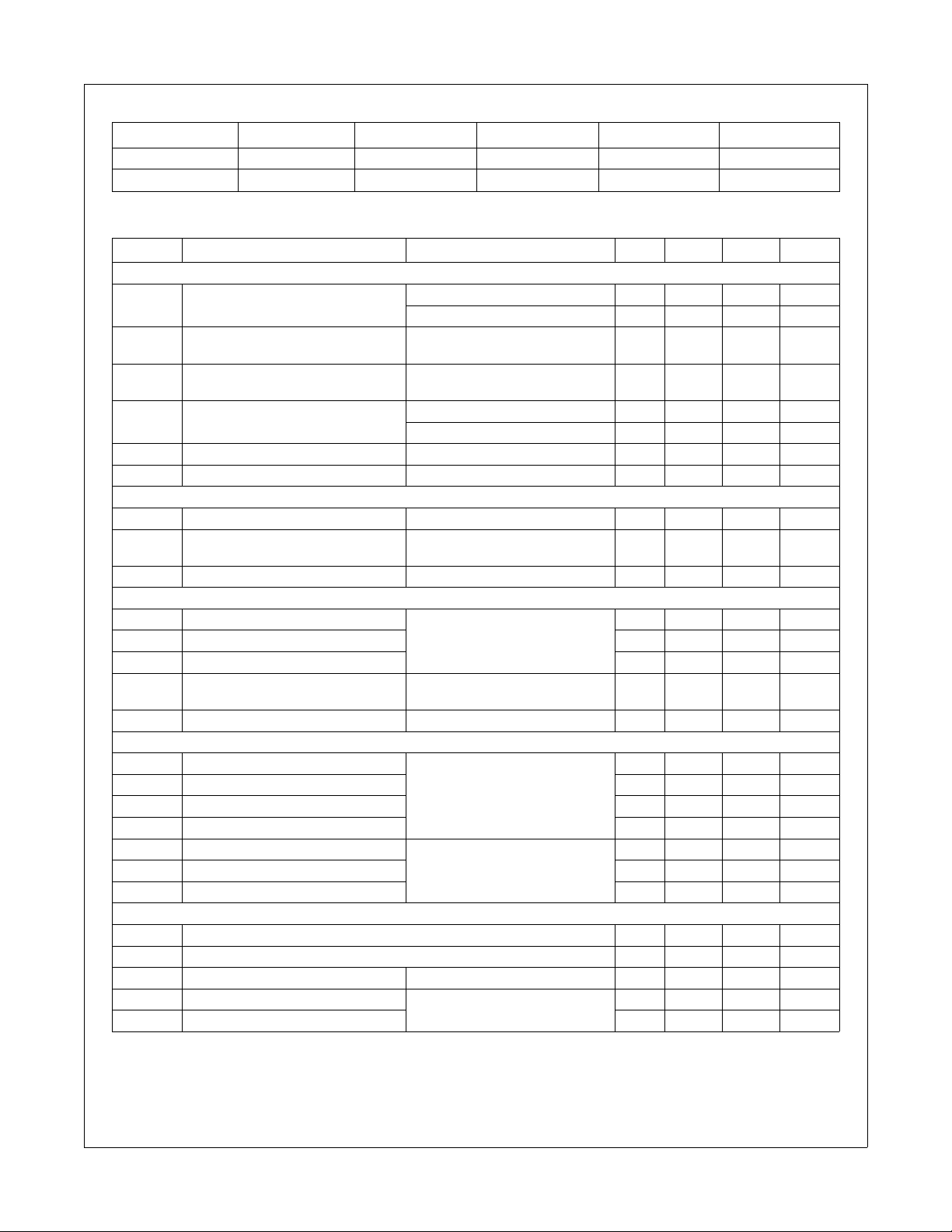
Typical Performance Characterist ics
Figure 1. On-Region Characteristics Figure 2. Transfer Characteristics
2
10
V
GS
Top : 15.0 V
10.0 V
8.0 V
7.0 V
6.5 V
1
10
6.0 V
Botto m : 5.5 V
0
10
, Drain Current [A]
D
I
-1
10
-1
10
VDS, Drain-Source Voltage [V]
Figure 3. On-Resistance Variation vs. Figure 4. Body Diode Forward Voltage
Drain Current and Gate Voltage Variation vs. Source Current
1
10
150oC
0
10
, Drain Current [A]
D
* Notes :
µ
s Pulse Test
1. 250
= 25oC
2. T
C
0
10
1
10
I
-1
10
246810
25oC
-55oC
* Note
1. V
2. 250
= 40V
DS
µ
s Pulse Test
VGS , Ga te -Sourc e Volta g e [V]
and Temperatue
FCP11N60F/FCPF11N60F 600V N-Channel MOSFET
25 oC
* Notes :
= 0V
1. V
GS
µ
s Pulse Test
2. 250
1.0
0.8
],
0.6
Ω
[
DS(ON)
R
0.4
0.2
Drain-Source On-Resistance
0.0
0 5 10 15 20 25 30 35 40
VGS = 10V
ID, Drain Cu rre n t [A]
VGS = 20V
* Note : TJ = 25oC
1
10
0
10
, Reverse Drain Current [A]
DR
I
-1
10
0.2 0.4 0.6 0.8 1.0 1.2 1.4 1.6
150 oC
VSD , Source-Drain Voltage [V]
Figure 5. Capacitance Characteristics Figure 6. Gate Charge Characteristics
6000
5000
4000
C
3000
2000
Capacitance [pF]
1000
0
-1
10
oss
C
iss
C
rss
0
10
C
= Cgs + Cgd (Cds = shorted)
iss
C
= Cds + C
oss
gd
C
= C
rss
gd
* Notes :
1. V
2. f = 1 MHz
1
10
= 0 V
GS
VDS, Drain-Source Voltage [V]
12
10
8
6
4
, Gate-Source Voltage [V]
2
GS
V
0
0 5 10 15 20 25 30 35 40 45
QG, Total Gate C h arg e [n C ]
VDS = 100V
VDS = 250V
VDS = 400V
* Note : ID = 11A
FCP11N60F/FCPF11N60F Rev. A1
3
www.fairchildsemi.com

FCP11N60F/FCPF11N60F 600V N-Channel MOSFET
Typical Performance Characterist ics
(Continued)
Figure 7. Breakdown Voltage Variation Figure 8. On-Resistance Variation
vs. Temperature vs. Temperature
1.2
1.1
1.0
, (Normalized)
BV
DSS
0.9
* Note s :
1. V
2. I
Drain-Source Breakdown Voltage
0.8
-100 -50 0 50 100 150 200
TJ, Junction Temperature [oC]
= 0 V
GS
= 250 µA
D
3.0
2.5
2.0
1.5
, (Normalized)
DS(ON)
1.0
R
Drain-Source On-Resistance
0.5
0.0
-100 -50 0 50 100 150 200
TJ, Junction Temperature [oC]
* Notes :
1. V
2. I
Figure 9-1. Safe Operating Area Figure 9-2. Safe Operating Area
for FCP11N60F for FCPF11N60F
2
10
Operation in This Are a
is Limited by R
1
10
0
10
2
10
Operation in This Area
1
10
is Limited by R
DS(on)
DS(on)
100 us
1 ms
10 ms
DC
0
10
1 ms
10 ms
100 ms
DC
= 10 V
GS
= 5.5 A
D
100 us
, Drain Current [A ]
* Notes :
D
-1
I
1. T
10
= 25 oC
C
= 150 oC
2. T
J
3. Single Pulse
-2
10
0
10
1
10
2
10
3
10
, Drain Current [A]
I
VDS, Drain-Source Voltage [V]
Figure 10. Maximum Drain Current vs. Case Temperature
12.5
10.0
7.5
5.0
, Drain Current [A]
D
I
2.5
0.0
25 50 75 100 125 150
TC, Case Temperature [oC]
D
-1
10
-2
10
10
* Notes :
= 25 oC
1. T
C
= 150 oC
2. T
J
3. Single Pulse
0
1
10
2
10
VDS, Drain-Source Voltage [V]
3
10
FCP11N60F/FCPF11N60F Rev. A1
4
www.fairchildsemi.com

FCP11N60F/FCPF11N60F 600V N-Channel MOSFET
Typical Performance Characterist ics
Figure 11-1. Transient Thermal Response Curve for FCP11N60F
0
10
D=0.5
0.2
0.1
-1
10
0.05
0.02
(t), Thermal Respons e
Z
Figure 11-2. Transient Thermal Response Curve for FCPF11N60F
(t), Thermal Response
Z
0.01
JC
θ
-2
10
-5
10
sin gle pulse
-4
10
t1, Square Wave Pulse Duration [sec]
D=0.5
0
10
0.2
0.1
0.05
-1
10
0.02
0.01
JC
θ
-2
10
-5
10
sing le p u ls e
-4
10
t1, Square Wave P ulse Duration [sec]
(Continued)
-3
10
-3
10
* Note s :
(t) = 1.0 oC/W Max.
1. Z
θ
JC
2. D u ty F ac to r, D = t
3. TJM - TC = PDM * Z
P
DM
-2
10
-1
10
1/t2
(t)
θ
JC
t
1
t
2
0
10
1
10
* Notes :
(t) = 3.5 oC/W Max.
1. Z
θ
JC
2. D u ty F a c to r , D = t
3. TJM - TC = PDM * Z
P
DM
-2
10
-1
10
1/t2
(t)
θ
JC
t
1
t
2
0
10
1
10
FCP11N60F/FCPF11N60F Rev. A1
5
www.fairchildsemi.com
12V
12V
200nF
200nF
3mA
3mA
50KΩ
50KΩ
V
V
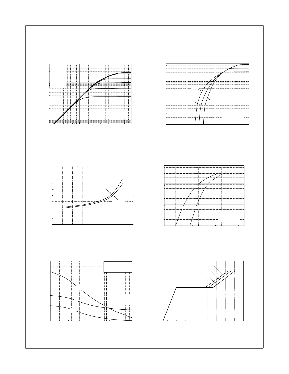
Gate Charge Test Circuit & Waveform
V
V
GS
GS
GS
300nF
300nF
Same Type
Same Type
as DUT
as DUT
DUT
DUT
V
V
DS
DS
GS
10V
10V
Resistive Switching Test Circuit & Waveforms
FCP11N60F/FCPF11N60F 600V N-Channel MOSFET
Q
Q
g
g
Q
Q
gs
gs
Q
Q
gd
gd
Charge
Charge
10V
10V
10V
10V
R
R
L
DUT
DUT
L
V
V
DD
DD
V
V
DS
DS
V
V
GS
GS
R
R
G
G
V
V
DS
DS
90%
90%
10%
10%
V
V
GS
GS
t
t
d(on)tr
d(on)tr
t
t
on
on
t
t
d(off)
d(off)
t
t
f
f
t
t
off
off
Unclamped Inductive Switching Test Circuit & Waveforms
BV
BV
DSS
L
LL
V
V
DS
DS
BV
BV
DSS
V
V
DSS
I
I
AS
AS
DD
DD
I
IDI
D
D
R
R
G
G
DUT
DUT
t
t
p
p
V
V
DD
DD
1
1
1
1
----
----
----
----
E
=LI
E
=LI
=LI
E
AS
AS
AS
2
2
2
2
2
2
2
AS
AS
AS
I
I
(t)
(t)
D
D
t
t
p
p
DSS
--------------------
-------------------BV
BV
DSS-VDD
DSS-VDD
Time
Time
V
(t)
V
(t)
DS
DS
FCP11N60F/FCPF11N60F Rev. A1
6
www.fairchildsemi.com

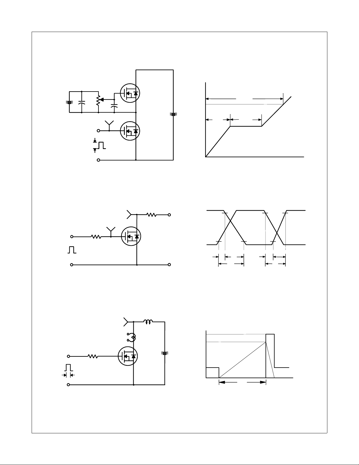
Peak Diode Recovery dv/dt Test Circuit & Waveforms
+
DUT
DUT
I
I
SD
SD
Driver
Driver
R
R
G
G
V
V
GS
GS
+
V
V
DS
DS
_
_
L
LL
Same Type
Same Type
as DUT
as DUT
• dv/dt controlled by R
• dv/dt controlled by R
•ISDcontroll ed by pulse period
•ISDcontroll ed by pulse period
G
G
FCP11N60F/FCPF11N60F 600V N-Channel MOSFET
V
V
DD
DD
V
V
GS
GS
( Driver )
( Driver )
I
I
SD
SD
( DUT )
( DUT )
V
V
DS
DS
( DUT )
( DUT )
Gate Pulse Width
Gate Pulse Width
Gate Pulse Width
--------------------------
--------------------------
--------------------------
D =
D =
D =
Gate Pulse Period
Gate Pulse Period
Gate Pulse Period
IFM, Body Diode Forward Current
IFM, Body Diode Forward Current
I
I
RM
RM
Body Diode Reverse Current
Body Diode Reverse Current
Body Diode Recoverydv/dt
Body Diode Recoverydv/dt
V
V
SD
SD
Body Diode
Body Diode
Forward Voltage Drop
Forward Voltage Drop
di/dt
di/dt
10V
10V
V
V
DD
DD
FCP11N60F/FCPF11N60F Rev. A1
7
www.fairchildsemi.com

Mechanical Dimensions
FCP11N60F/FCPF11N60F 600V N-Channel MOSFET
TO - 220
FCP11N60F/FCPF11N60F Rev. A1
Dimensions in Millimeters
8
www.fairchildsemi.com

FCP11N60F/FCPF11N60F 600V N-Channel MOSFET
Mechanical Dimensions
10.16 ±0.20
3.30 ±0.10
15.80 ±0.20
(Continued)
(7.00)
TO-220F
ø3.18 ±0.10
6.68 ±0.20
(1.00x45°)
2.54
(0.70)
±0.20
15.87 ±0.20
9.75 ±0.30
MAX1.47
0.80 ±0.10
0.35 ±0.10
2.54TYP
[2.54
±0.20]
#1
9.40 ±0.20
(30°)
2.54TYP
[2.54
±0.20]
4.70 ±0.20
0.50
+0.10
–0.05
2.76 ±0.20
FCP11N60F/FCPF11N60F Rev. A1
Dimensions in Millimeters
9
www.fairchildsemi.com

TRADEMARKS
The following includes registered and unregistered trademarks and se rvice marks, owned by Fairchild Semiconductor and/or its global subsidiarie s, and i s not
intended to be an exhaustive list of all such trademarks.
Build it Now™
CorePLUS™
CorePOWER™
CROSSVOLT™
CTL™
Current Transfer Logic™
EcoSPARK
EfficentMax™
EZSWITCH™ *
™
Fairchild
Fairchild Semiconductor
FACT Quiet Series™
FACT
FAST
FastvCore™
FlashWriter
FPS™
®
®
tm
®
®
®
®
*
®
F-PFS™
* EZSWITCH™ and FlashWriter
®
are trademarks of System General Corporation, used under license by Fairchild Semiconductor.
®
FRFET
Global Power Resource
Green FPS™
Green FPS™ e-Series™
GTO™
IntelliMAX™
ISOPLANAR™
MegaBuck™
MICROCOUPLER™
MicroFET™
MicroPak™
MillerDrive™
MotionMax™
Motion-SPM™
OPTOLOGIC
OPTOPLANAR
PDP SPM™
Power-SPM™
PowerTrench
PowerXS™
®
®
tm
®
®
SM
Programmable Active Droop™
®
QFET
QS™
Quiet Series™
RapidConfigure™
™
Saving our world, 1mW /W /kW at a time™
SmartMax™
SMART START™
®
SPM
STEALTH™
SuperFET™
SuperSOT™-3
SuperSOT™-6
SuperSOT™-8
SupreMOS™
SyncFET™
®
The Power Franchise
®
TinyBoost™
tm
TinyBuck™
®
TinyLogic
TINYOPTO™
TinyPower™
TinyPWM™
TinyWire™
μSerDes™
®
UHC
Ultra FRFET™
UniFET™
VCX™
VisualMax™
XS™
DISCLAIMER
FAIRCHILD SEMICONDUCTOR RESERVES THE RIGHT TO MAKE CHANGES WITHOUT FURTHER NOTICE TO ANY PRODUCTS HEREIN TO IMPROVE
RELIABILITY, FUNCTION, OR DESIGN. FAIRCHILD DOES NOT ASSUME ANY LIABILITY ARISING OUT OF THE APPLICATION OR USE OF ANY
PRODUCT OR CIRCUIT DESCRIBED HEREIN; NEITHER DOES IT CONVEY ANY LICENSE UNDER ITS PATENT RIGHTS, NOR THE RIGHTS OF OTHERS.
THESE SPECIFICATIONS DO NOT EXPAND THE TERMS OF FAIRCHILD’S WORLDWIDE TERMS AND CONDITIONS, SPECIFICALLY THE WARRANTY
THEREIN, WHICH COVERS THESE PRODUCTS.
FCP11N60F/FCPF11N60F 600V N-Channel MOSFET
LIFE SUPPORT POLICY
FAIRCHILD’S PRODUCTS ARE NOT AUTHORIZED FOR USE AS CRITICAL COMPONENTS IN LIFE SUPPORT DEVICES OR SYSTEMS WITHOUT THE
EXPRESS WRITTEN APPROVAL OF FAIRCHILD SEMICONDUCTOR CORPORATION.
As used herein:
1. Life support devices or systems are devices or systems which, (a) are
intended for surgical implant into the body or (b ) support or sustain li fe,
and (c) whose failure to perform when properly u sed in accordance with
instructions for use provided in the labeling, can be reasonably
expected to result in a significant injury of the user.
ANTI-COUNTERFEITING POLICY
Fairchild Semiconductor Corporation’s Anti-Counterfeiting Policy. Farichild’s Anti-Counterfeiting Policy is also stated on our external website,
www.fairchildsemi.com, under Sales Support
.
2. A critical component in any component of a life support, device, or
system whose failure to perform can be reasonably expected to cause
the failure of the life support device or system, or to affect its safety or
effectiveness.
Counterfeiting of semiconductor parts is a growing problem in the industry. All man ufactures of semiconduct or products are exp eriencing counterf eiting of their
parts. Customers who inadvertently purchase counterfeit parts experience many pro blems such as loss of brand re putat ion, subst andar d per fo rmance, fa iled
application, and increased cost of production and manufacturing delays. Fairchild is taking strong measures to protect ourselves and our customers from the
proliferation of counterfeit parts. Farichild str ongly encourag es cu stomers to pu rchase Farichild pa rts either dire ctly from Fairchil d or from Authorized Fairchild
Distributors who are listed by country on our web page cited above. Products customers buy either from fairchild directly or from Authorized Fairchild
Distributors are genuine parts, have full traceability, meet Fairchild’s quality standards for handing and storage and provide access to Farichild’s full range of
up-to-date technical and product information. Fairchild and our Authorized Distributors will stand behind all warranties and will appropriately address and
warranty issues that may arise. Fairchild will not provide any warranty coverage or other assistance for parts bought from Unauthorized Sources. Farichild is
committed to combat this global problem and encourage our customers to do their part in st opping this practice by buying d irect or from authorized distri butors.
PRODUCT STATUS DEFINITIONS
Definition of Terms
Datasheet Identification Product Status Definition
Advance Information Formative / In Design
Preliminary First Production
No Identification Needed Full Production
Obsolete Not In Production
Datasheet contains the design specifications for product development. Specifications
may change in any manner without notice.
Datasheet contains preliminary data; supplementary data will be published at a later
date. Fairchild Semiconductor reserves the right to make changes at any time without
notice to improve design.
Datasheet contains final specifications. Fairchild Semiconductor reserves the right to
make changes at any time without notice to improve the design.
Datasheet contains specifications on a product that is discontinu ed by Fairchild
Semiconductor. The datashe et is for reference information only.
Rev. I37
FCP11N60F/FCPF11N60F Rev. A1
10
www.fairchildsemi.com
 Loading...