FCH35N60
600V N-Channel MOSFET
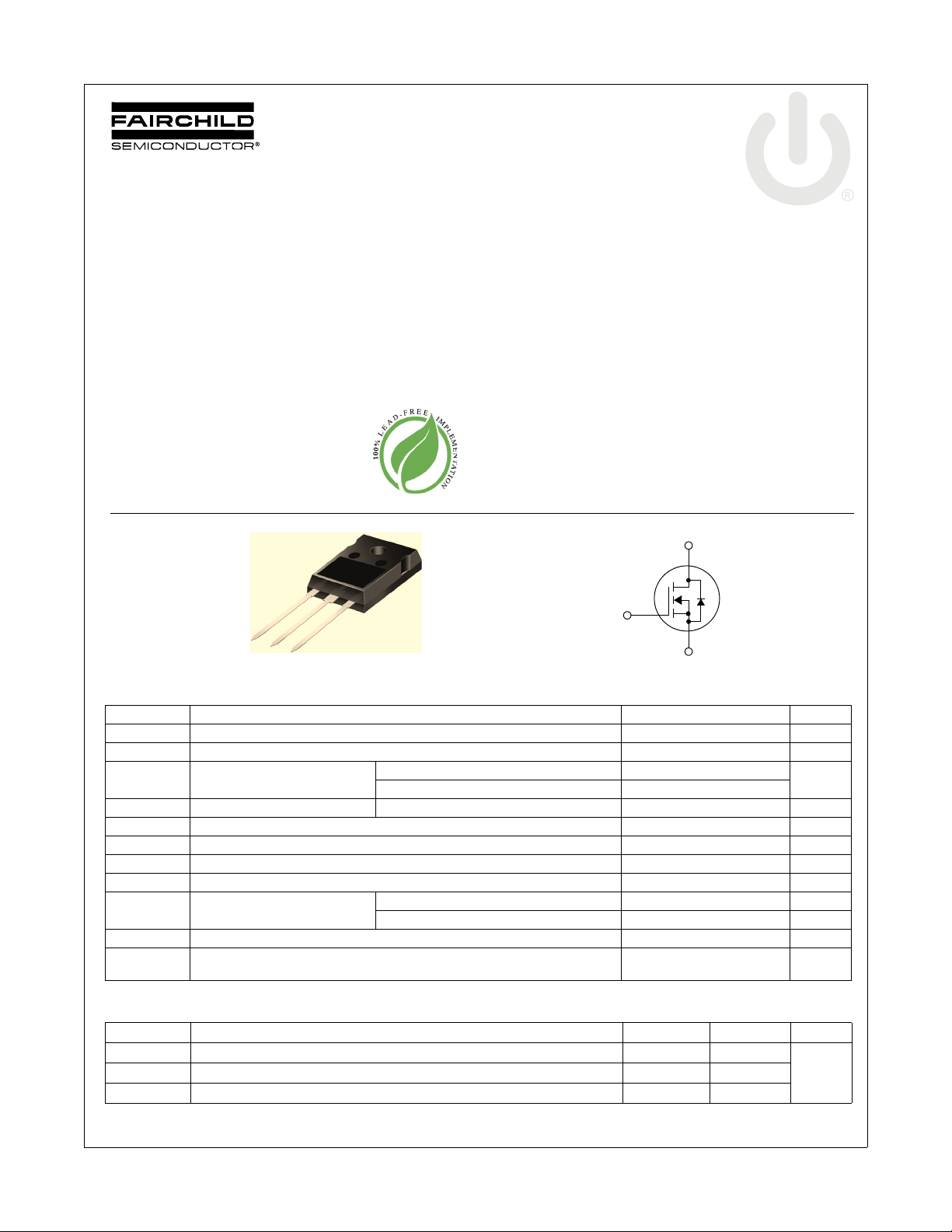
FCH35N60 N-Channel MOSFET
February 2010
TM
SuperFET
Features
• 650V @ TJ = 150°C
•Typ.R
• Ultra low gate charge ( Typ. Q
• Low effective output capacitance ( Typ. C
• 100% avalanche tested
MOSFET Maximum Ratings T
Symbol Parameter Ratings Units
V
DSS
V
GSS
I
D
I
DM
E
AS
I
AR
E
AR
dv/dt Peak Diode Recovery dv/dt (Note 3) 20 V/ns
P
D
, T
T
J
STG
T
L
*Drain current limited by maximum junction temperature
= 0.079Ω
DS(on)
= 139nC )
g
.eff = 340pF )
oss
G
D
S
Drain to Source Voltage 600 V
Gate-Soure voltage ±30 V
D r a i n C u r r e n t
D r a i n C u r r e n t - P u l s e d (Note 1) 105 A
Single Pulsed Avalanche Energy (Note 2) 1455 mJ
Avalanche Current (Note 1) 35 A
Repetitive Avalanche Energy (Note 1) 31.25 mJ
Power Dissipation
Operating and Storage Temperature Range -55 to +150
Maximum Lead Temperature for Soldering Purpose,
1/8” from Case for 5 Seconds
TO-247
= 25oC unless otherwise noted*
C
-Continuous (T
-Continuous (T
(T
= 25oC) 312.5 W
C
- Derate above 25
Description
SuperFETTM is Farichild’s proprietary, new generation of high
voltage MOSFET family that is utilizing an advanced charge
balance mechanism for outstanding low on-resistance and lower
gate charge performance.
This advanced technology has been tailored to minimize
conduction loss, provide superior switching performance, and
withstand extreme dv/dt rate and higher avalanche energy.
Consequently, SuperFET is very suitable for various AC/DC
power conversion in switching mode operation for system
miniaturization and higher efficiency.
D
G
S
= 25oC) 35
C
= 100oC) 22.2
C
o
C2.5W/
300
o
o
Thermal Characteristics
Symbol Parameter Typ. Max. Units
R
θJC
θCS
R
θJA
Thermal Resistance, Junction to Case - 0.4
Thermal Resistance, Case-to-Heat Sink 0.24 -
Thermal Resistance, Junction to Ambient - 42
o
C/WR
A
o
C
C
C
©2010 Fairchild Semiconductor Corporation
FCH35N60 Rev. A1
www.fairchildsemi.com1

FCH35N60 N-Channel MOSFET
Package Marking and Ordering Information T
= 25oC unless otherwise noted
C
Device Marking Device Package Reel Size Tape Width Quantity
FCH35N60 FCH35N60 TO-247 - - 30
Electrical Characteristics
Symbol Parameter Test Conditions Min. Typ. Max. Units
Off Characteristics
I
= 250μA, VGS = 0V, TJ = 25oC 600 - - V
BV
DSS
ΔBV
/ ΔT
BV
DS
I
DSS
I
GSS
DSS
J
Drain to Source Breakdown Voltage
Breakdown Voltage Temperature
Coefficient
Drain-Source Avalanche Breakdown
Voltage
Zero Gate Voltage Drain Current
Gate to Body Leakage Current VGS = ±30V, V
On Characteristics
V
GS(th)
R
DS(on)
g
FS
Gate Threshold Voltage VGS = VDS, ID = 250μA3.0-5.0V
Static Drain to Source On Resistance VGS = 10V, ID = 17.5A - 0.079 0.098 Ω
Forward Transconductance VDS = 40V, ID = 17.5A - 28.8 - S
Dynamic Characteristics
C
iss
C
oss
C
rss
C
oss
eff. Effective Output Capacitance VDS = 0V to 480V, VGS = 0V - 340 - pF
C
oss
Q
g
Q
gs
Q
gd
ESR Equivalent Series Resistance (G-S) Drain Open, F= 1MHZ - 1.4 - Ω
Input Capacitance
Output Capacitance - 2380 3170 pF
Reverse Transfer Capacitance - 140 - pF
Output Capacitance VDS = 480V, VGS = 0V, f = 1.0MHz - 113 - pF
Total Gate Charge at 10V
Gate to Source Gate Charge - 31 - nC
Gate to Drain “Miller” Charge - 69 - nC
D
= 250μA, VGS = 0V, TJ = 150oC- 650 - V
I
D
I
= 250μA, Referenced to 25oC-0.6-V/
D
V
= 0V, ID = 16A - 700 - V
GS
V
= 600V, V
DS
= 480V, TC = 125oC--10
V
DS
= 25V, VGS = 0V
V
DS
f = 1MHz
= 0V - - 1
GS
= 0V - - ±100 nA
DS
- 4990 6640 pF
- 139 181 nC
V
= 480V, ID = 35A
DS
V
= 10V
GS
(Note 4)
μA
o
C
Switching Characteristics
t
d(on)
t
r
t
d(off)
t
f
Turn-On Delay Time
Turn-On Rise Time - 120 250 ns
Turn-Off Delay Time - 105 220 ns
Turn-Off Fall Time - 73 155 ns
Drain-Source Diode Characteristics
I
S
I
SM
V
SD
t
rr
Q
rr
Notes:
1: Repetitive Rating: Pulse width limited by maximum junction temperature
= 17.5A, VDD = 50V, RG = 25Ω, Starting TJ = 25°C
2: I
AS
3: I
≤ 35A, di/dt ≤ 200A/μs, VDD ≤ BV
SD
4: Essentially Independent of Operating Temperature Typical Characteristics
FCH35N60 Rev. A1
Maximum Continuous Drain to Source Diode Forward Current - - 35 A
Maximum Pulsed Drain to Source Diode Forward Current - - 105 A
Drain to Source Diode Forward Voltage V
Reverse Recovery Time
Reverse Recovery Charge - 16.3 - μC
, Starting TJ = 25°C
DSS
= 300V, ID = 35A
V
DD
R
= 4.7Ω
G
(Note 4)
= 0V, I
GS
= 0V, I
V
GS
dI
/dt = 100A/μs
F
= 35A - - 1.4 V
SD
= 35A
SD
2
-3478ns
- 614 - ns
www.fairchildsemi.com

Typical Performance Characteristics
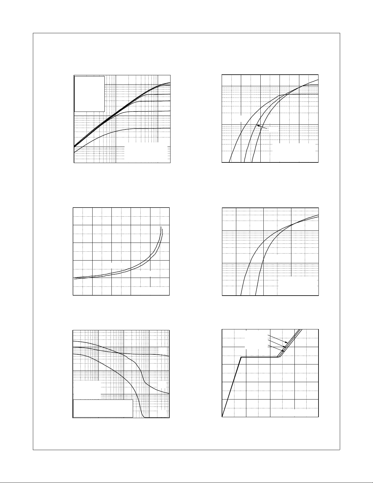
Figure 1. On-Region Characteristics Figure 2. Transfer Characteristics
200
V
= 15.0 V
GS
100
10.0 V
8.0 V
7.0 V
6.5 V
6.0 V
5.5 V
10
, Drain Current[A]
D
I
1
0.3
0.1 1 10 20
*Notes:
1. 250
2. T
μs Pulse Test
= 25oC
C
VDS, Drain-Source Voltage[V]
Figure 3. On-Resistance Variation vs. Figure 4. Body Diode Forward Voltage
Drain Current and Gate Voltage Variation vs. Source Current
and Temperature
0.24
200
100
10
, Drain Current[A]
D
I
1
150oC
456789
-55oC
25oC
*Notes:
1. V
2. 250
= 20V
DS
μs Pulse Test
VGS, Gate-Source Voltage[V]
500
FCH35N60 N-Channel MOSFET
0.20
100
0.16
[Ω],
0.12
DS(ON)
R
0.08
VGS = 10V
VGS = 20V
Drain-Source On-Resistance
0.04
0 255075100125
*Note: TC = 25oC
ID, Drain Current [A]
10
, Reverse Drain Current [A]
S
I
1
150oC
25oC
*Notes:
1. VGS = 0V
2. 250
μs Pulse Test
0.2 0.4 0.8 1.2 1.6
VSD, Body Diode Forward Voltage [V]
Figure 5. Capacitance Characteristics Figure 6. Gate Charge Characteristics
50000
10000
1000
*Note:
1. V
= 0V
100
Capacitances [pF]
10
GS
2. f = 1MHz
C
= Cgs + Cgd (Cds = shorted)
iss
C
= Cds + C
oss
C
rss
= C
gd
gd
0.1 1 10 100 600
VDS, Drain-Source Voltage [V]
C
iss
C
oss
C
rss
10
VDS = 100V
= 250V
V
DS
= 400V
V
8
DS
6
4
, Gate-Source Voltage [V]
GS
V
2
0
04080120160
*Note: ID = 35A
Qg, Total Gate Charge [nC]
FCH35N60 Rev. A1
3
www.fairchildsemi.com
 Loading...