Fairchild FAN5602 service manual

August 2009
FAN5602 — Universal (Step-Up/Step-Down) Charge
Pump Regulated DC/DC Converter
FAN5602 — Universal (Step-Up/Step-Down) Charge Pump Regulated DC/DC Converter
Features
■
Low-Noise, Constant-Frequency Operation at Heavy Load
■
High-Efficiency, Pulse-Skip (PFM) Operation at Light Load
■ Switch Configurations (1:3, 1:2, 2:3, 1:1, 3:2, 2:1, 3:1)
■ 92% Peak Efficiency
■ Input Voltage Range: 2.7V to 5.5V
■ Output Current: 4.5V, 100mA at V
■ ±3% Output Voltage Accuracy
■ I
< 1µA in Shutdown Mode
CC
■ 1MHz Operating Frequency
■ Shutdown Isolates Output from Input
■ Soft-Start Limits Inrush Current at Startup
■ Short-Circuit and Over-Temperature Protection
■ Minimum External Component Count
■ No Inductors
= 3.6V
IN
Applications
■ Cell Phones
■ Handheld Computers
■ Portable RF Communication Equipment
■ Core Supply to Low-Power Processors
■ Low-Voltage DC Bus
■ DSP Supplies
Description
The FAN5602 is a universal switched capacitor DC/DC
converter capable of step-up or step-down operation.
Due to its unique adaptive fractional switching topology,
the device achieves high efficiency over a wider input/
output voltage range than any of its predecessors. The
FAN5602 utilizes resistance-modulated loop control,
which produces lower switching noise than other topologies. Depending upon actual load conditions, the device
automatically switches between constant-frequency and
pulse-skipping modes of operation to extend battery life.
The FAN5602 produces a fixed regulated output within
the range of 2.7V to 5.5V from any type of voltage
source. High efficiency is achieved under various input/
output voltage conditions because an internal logic circuit
automatically reconfigures the system to the best possible topology. Only two 1µF bucket capacitors and one
10µF output capacitor are needed. During power on,
soft-start circuitry prevents excessive current drawn from
the supply. The device is protected against short-circuit
and over-temperature conditions.
The FAN5602 is available with 4.5V and 5.0V output voltages in a 3x3mm 8-lead MLP package.
Ordering Information
Part Number Package Eco Status Output Voltage, N
FAM6502MP45X 3x3mm 8-Lead MLP Green 4.5V
FAN5602MP5X 3x3mm 8-Lead MLP Green 5.0V
Note:
1. Reference MLP08D Option B ONLY.
2. For Fairchild’s definition of “green” Eco Status, please visit: http://www.fairchildsemi.com/company/green/rohs_green.html
VOM
.
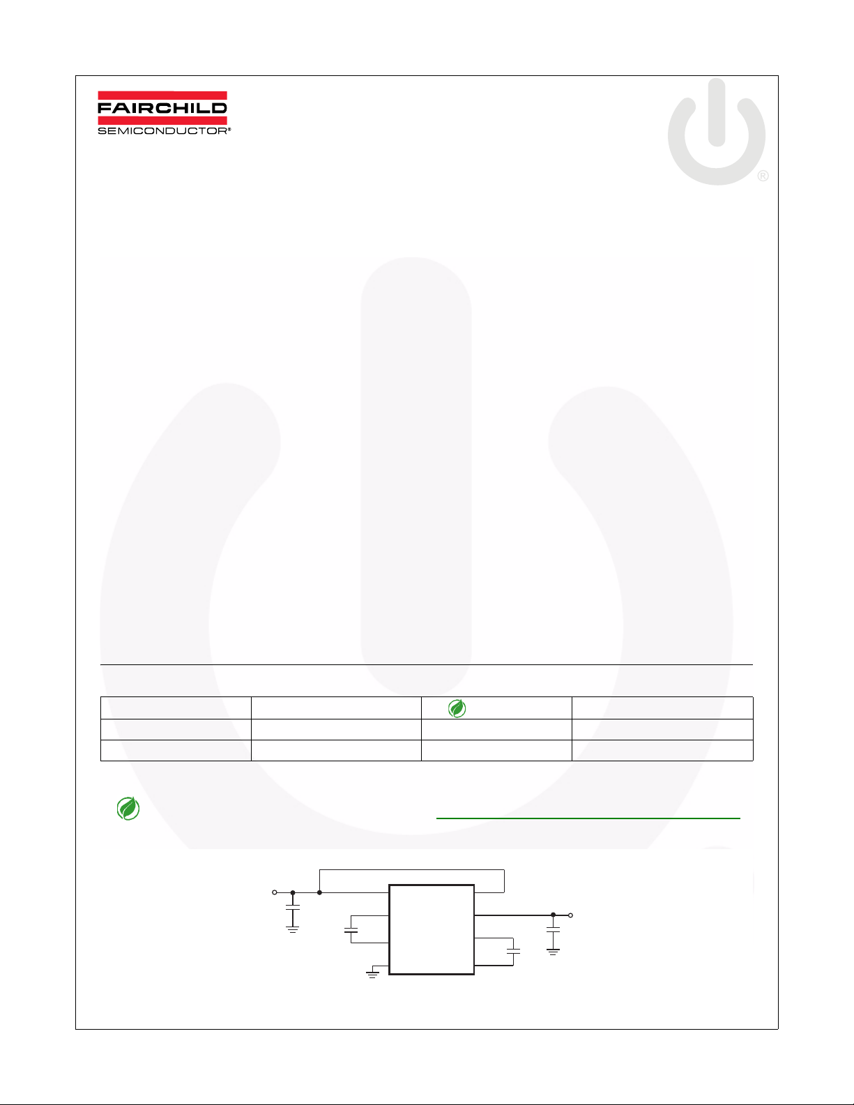
Application Diagram
Input 2.7V to 5.5V
V
IN
1
C
B
GND
C2+
C2-
2
FAN5602
3
4
C
IN
8
6
7
5
Figure 1. Typical Application Diagram
© 2005 Fairchild Semiconductor Corporation www.fairchildsemi.com
FAN5602 Rev. 1.5.3
C1+
C1-
ENABLE
C
V
OUT
OUT

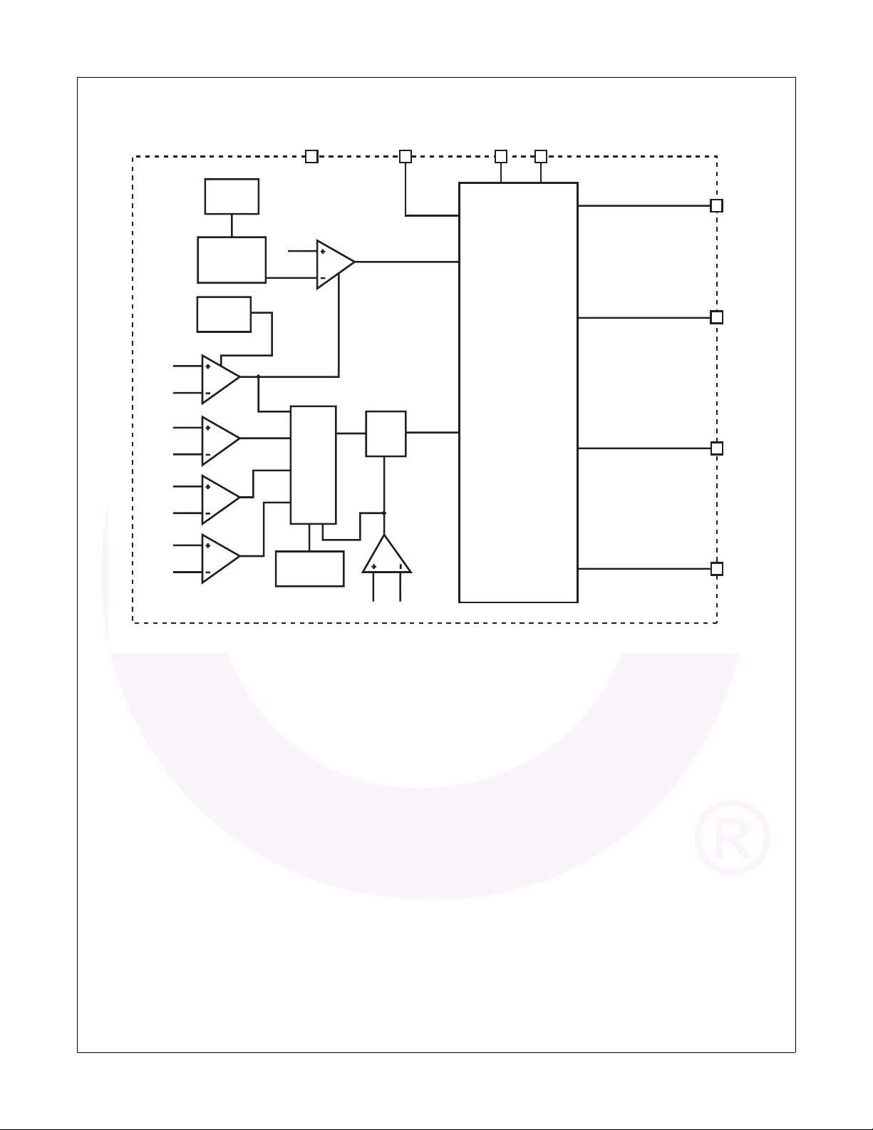
Block Diagram
ENABLE
FAN5602 — Universal (Step-Up/Step-Down) Charge Pump Regulated DC/DC Converter
V
IN
C1+C1-
FB
BG
REF
V
IN
150mV
V
OUT
1.6V
V
IN
BAND GAP
SOFT-START
CURRENT
SENSE
Light load
EN
PFM
MODE
SC
UVLO
FB
ERROR
AMP
BG
Heavy Load
CONTROL LOGIC
OSCILLATOR
EN
V
IN V
DRIVER
OUT
S
W
I
T
C
H
A
R
R
A
Y
V
OUT
C2+
C2-
GND
Figure 2. Block Diagram
© 2005 Fairchild Semiconductor Corporation www.fairchildsemi.com
FAN5602 Rev. 1.5.3 2

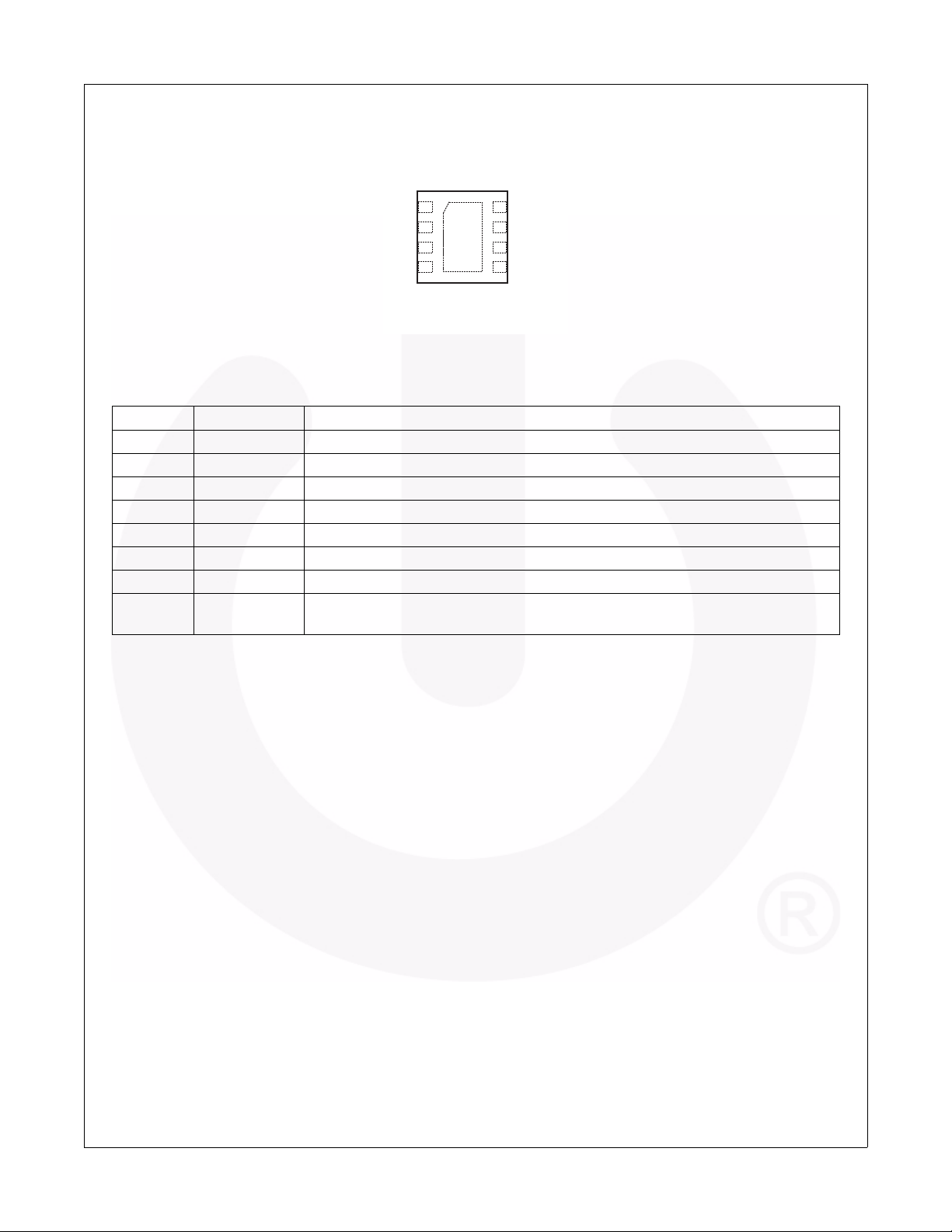
Pin Assignments
V
IN
C2+
C2-
GND
1
2
3
4 5
8
7
6
ENABLE
C1+
V
OUT
C1-
3x3mm 8-Lead MLP
Figure 3. Pin Assignments
Pin Descriptions
Pin # Name Description
1VINSupply Voltage Input.
2 C2+ Bucket Capacitor2. Positive Connection.
3 C2- Bucket Capacitor2. Negative Connection.
4 GND Ground
5 C1- Bucket Capacitor1. Negative Connection.
6V
OUT
7 C1+ Bucket Capacitor1. Positive Connection.
8 ENABLE
Regulated Output Voltage. Bypass this pin with 10μF ceramic low-ESR capacitor.
Enable Input. Logic high enables the chip and logic low disables the chip, reducing the
supply current to less than 1µA. Do not float this pin.
FAN5602 — Universal (Step-Up/Step-Down) Charge Pump Regulated DC/DC Converter
© 2005 Fairchild Semiconductor Corporation www.fairchildsemi.com
FAN5602 Rev. 1.5.3 3

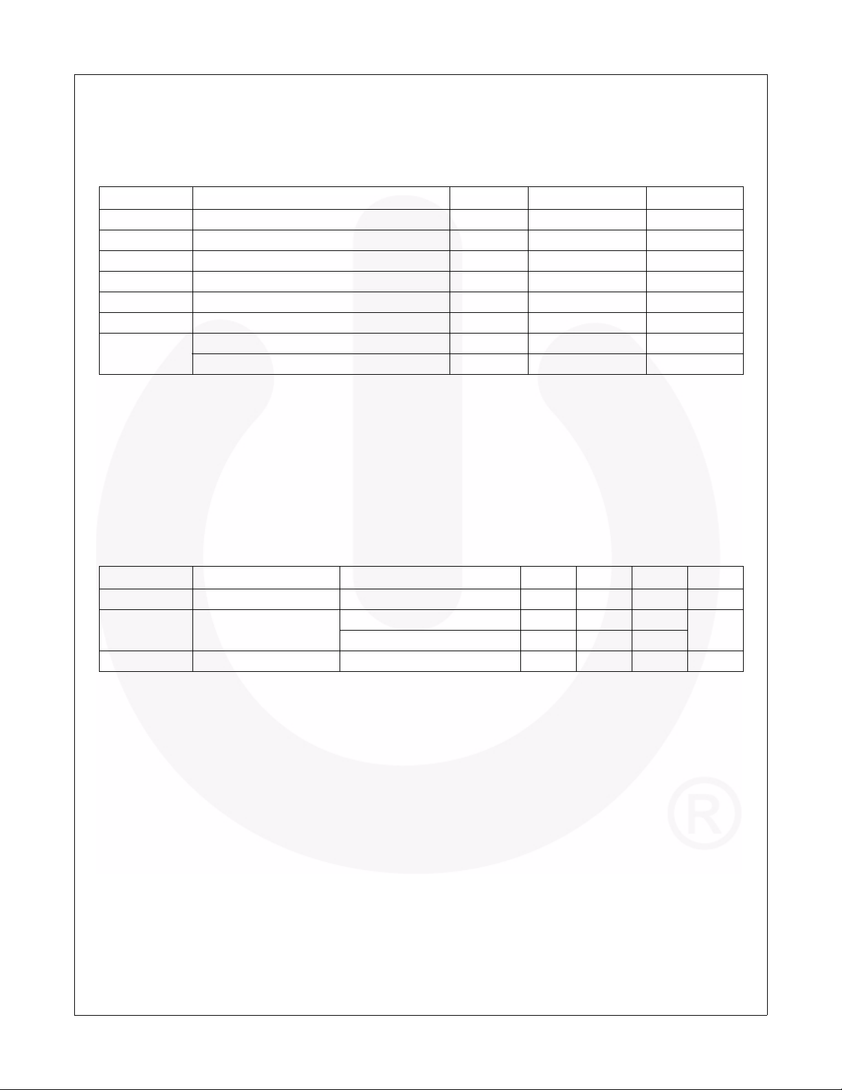
Absolute Maximum Ratings
Stresses exceeding the absolute maximum ratings may damage the device. The device may not function or be operable above the recommended operating conditions and stressing the parts to these levels is not recommended. In addition, extended exposure to stresses above the recommended operating conditions may affect device reliability. The
absolute maximum ratings are stress ratings only.
Symbol Parameter Min. Max. Unit
V
IN
P
D
T
L
T
J
T
STG
ESD
Note:
2. Using Mil Std. 883E, method 3015.7 (Human Body Model) and EIAJ/JESD22C101-A (Charged Device Model).
V
IN, VOUT,
Voltage at C1+,C1-,C2+, and C2-to GND -3.0 V
ENABLE, Voltage to GND -3.0 6.0 V
+0.3 V
IN
Power Dissipation Internally Limited
Lead Soldering Temperature (10 seconds) 300 C°
Junction Temperature 150 C°
Storage Temperature -55 150 C°
Human Body Model (HBM) 2 kV
Charged Device Model (CDM) 2 kV
FAN5602 — Universal (Step-Up/Step-Down) Charge Pump Regulated DC/DC Converter
Recommended Operating Conditions
The Recommended Operating Conditions table defines the conditions for actual device operation. Recommended
operating conditions are specified to ensure optimal performance to the datasheet specifications. Fairchild does not
recommend exceeding them or designing to Absolute Maximum Ratings.
Symbol Parameter Condition Min. Typ. Max. Unit
V
IN
I
L
T
A
Note:
3. Refer to Figure 9 in Typical Performance Characteristics.
Input Voltage 1.8 5.5 V
Load Current
VIN < 2V 30
4.5 & 5.5,V
= 3.6V 100
IN
mA
Ambient Temperature -40 +85 C°
© 2005 Fairchild Semiconductor Corporation www.fairchildsemi.com
FAN5602 Rev. 1.5.3 4
 Loading...