Fairchild FAN5601 service manual
■
■
■
■
■
■
■
■ 30 µ
■
■
■
■
■
■
■
■
■
■
■
■
■
■
FAN5601 Regulated Step-Down Charge Pump DC/DC Converter
July 2005
FAN5601
Regulated Step-Down Charge Pump DC/DC Converter
Features
> 85% Peak Efficiency
Low EMI
Low Ripple
Output Voltage 1.3V/1.8V
Input Voltage Range: 2.2V to 5.5V
Output Current: Up to 250mA
±2.5% Output Voltage Accuracy
A Operating Current
I
< 1 µ A in Shutdown Mode
CC
2MHz Operating Frequency
Shutdown Isolates Output from Input
Soft-Start Limits Inrush Current
Short Circuit and Over Temperature Protection
Minimum External Component Count
6-Lead 3x3mm MLP Package
Applications
Cell Phones
Handheld Computers
Por table Electronic Equipment
Core Supply to Next Generation Processors
Low Voltage DC Bus
Digital Cameras
DSP Supplies
Description
The FAN5601 is an advanced third generation switched capacitor step down DC/DC converter utilizing Fairchild’s proprietary
ScalarPump™ technology. This innovative architecture utilizes
scalar switch re-configuration and fractional switching techniques to produce low output ripple, low ESR spikes and
improve efficiency over a wide load range.
The FAN5601 produces a fixed regulated output from 2.2V to
5V input voltage. Customized output voltages are available in
100mV increments from 1V to 1.8V. Contact marketing for customized outputs.
In order to maximize efficiency, the FAN5601 achieves
regulation by skipping pulses. Depending upon load current, the
size of the switches is scaled dynamically, consequently, current
spikes and EMI are minimized. An internal soft start circuitry
prevents excessive current drawn from the supply. The device is
internally protected against short circuit and over temperature
conditions.
The FAN5601 is available in 6-lead 3x3mm MLP.
ScalarPump
™
is a registered trademark of Fairchild Semiconductor Corporation.
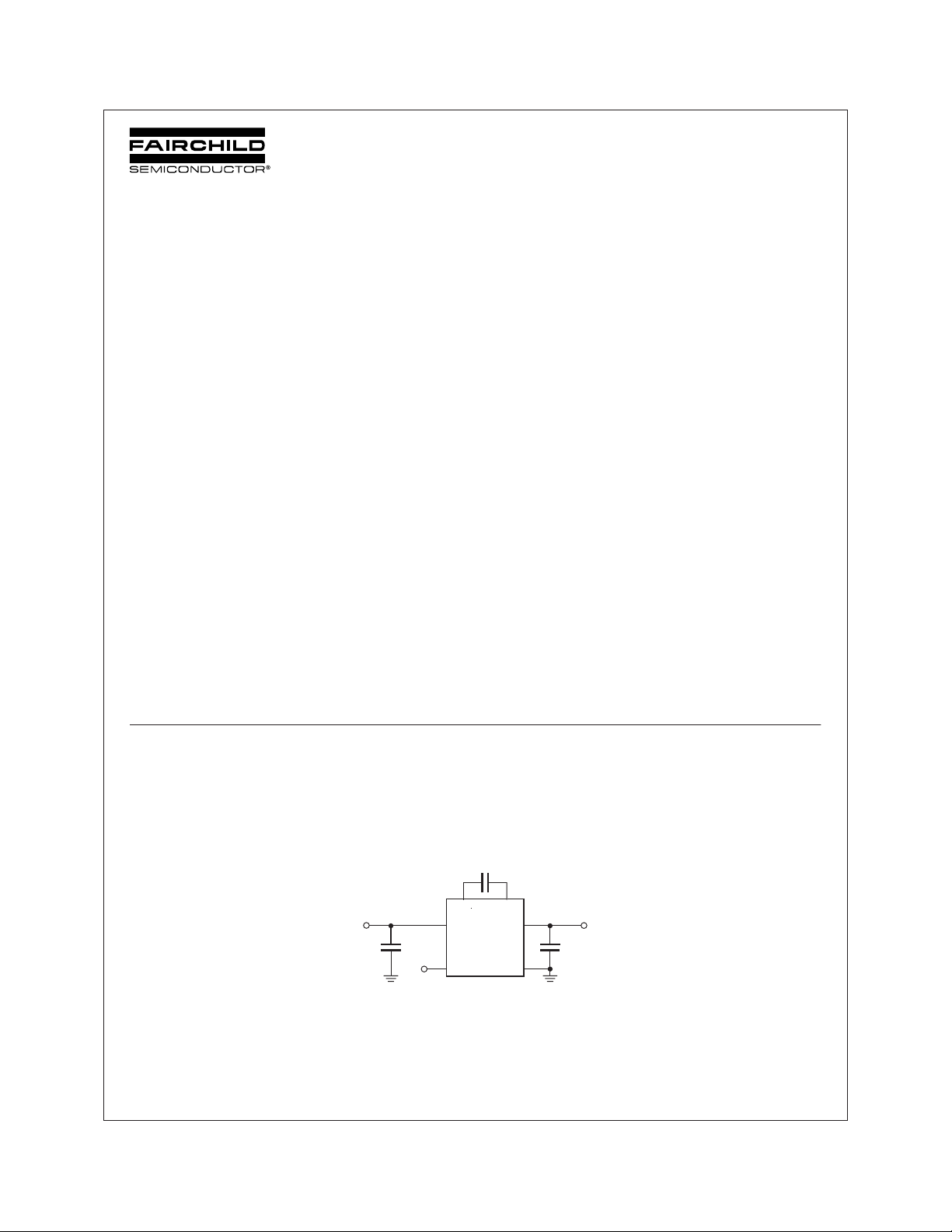
Typical Application
©2005 Fairchild Semiconductor Corporation
FAN5601 Rev. 1.0.5
INPUT 2.2V to 5.5V
= 10µF
C
IN
CB = 1µF
C+ C-
V
IN
ENABLE
1
OUTPUT 1.0V to 1.8V
V
OUT
FAN5601
GND
C
OUT
= 10µF
www.fairchildsemi.com
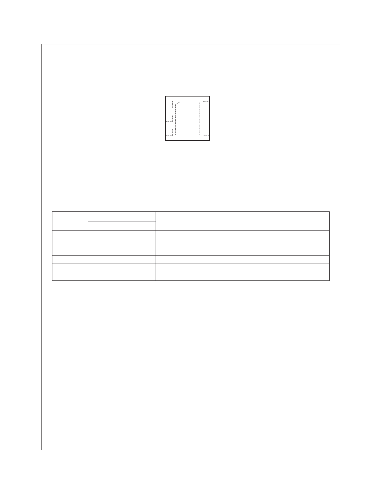
Pin Assignment
FAN5601 Regulated Step-Down Charge Pump DC/DC Converter
FAN5601
Top-View
1
C+
2
C-
ENABLE
3
6-Lead 3x3mm MLP
Pin Description
Pin Name
Pin No.
1C+Bucket Capacitor Positive Connection
2C-Bucket Capacitor Negative Connection
3 ENABLE Enable Pin
4 GND Ground
5V
6V
OUT
IN
Regulated Output Voltage. Bypass this pin with 10µF ceramic low ESR capacitor.
Supply Voltage Input
V
6
IN
V
5
OUT
4
GND
Pin Function Description6-Lead 3x3mm MLP
FAN5601 Rev. 1.0.5
2
www.fairchildsemi.com
FAN5601 Regulated Step-Down Charge Pump DC/DC Converter
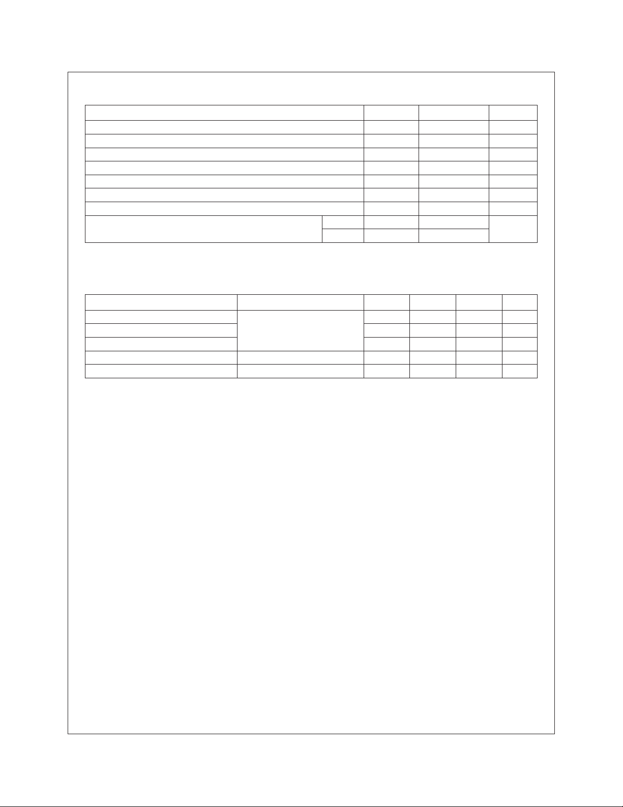
Absolute Maximum Ratings
(Note1)
Parameter Min Max Unit
V
,V
, ENABLE to GND -0.3 6.0 V
IN
OUT
C+, C-, to GND -0.3 V
V
Short Circuit Duration INDEFINITE
OUT
Lead Soldering Temperature (10 seconds) 300 °C
Operating Temperature Range -40 +85 °C
Junction Temperature 150 °C
Storage Temperature -55 150 °C
Electrostatic Discharge (ESD) Protection (Note2) HBM 4 kV
CDM 1
+ 0.3 V
IN
Recommended Operating Conditions
Parameter Package Min Typ Max Unit
Input Voltage 2.2 5.5 V
Output Current 250 mA
Operating Ambient Temperature -40 85 °C
Thermal Resistance Junction to Tab 6-lead 3x3mm MLP 8 °C/W
Thermal Resistance Junction to Ambient 6-lead 3x3mm MLP (Note 3) 90 °C/W
Notes:
1. Operation beyond the absolute maximum rating may cause permanent damage to device.
2. Using Mil Std. 883E, method 3015.7(Human Body Model) and EIA/JESD22C101-A (Charge Device Model).
3. One square inch, 1oz bottom side GND plane connected to top side GND plane by field of via.
FAN5601 Rev. 1.0.5
3
www.fairchildsemi.com
µ
µ
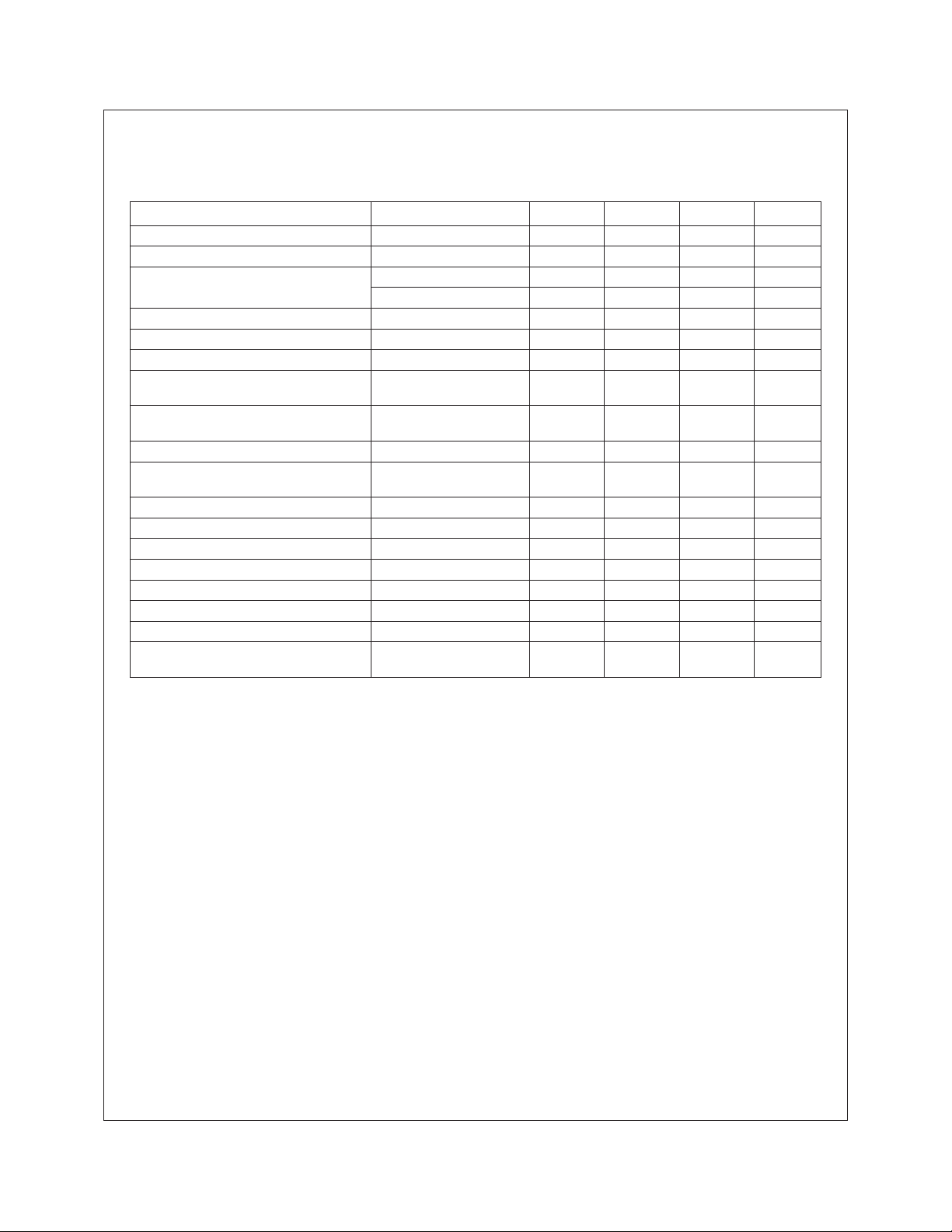
Electrical Characteristics
V
= 2.2V to 5.5V, I
IN
measured at T
= 25°C, unless otherwise noted.
A
Parameter Conditions Min. Typ. Max. Units
Input Undervoltage Lockout 1.9 2.0 2.17 V
Output Voltage Vnom V
Output Voltage Accuracy T
Output Voltage Temperature Coefficient V
Load Regulation 0.133 mV/mA
Line Regulation T
No load Supply Current (Note 4) I
Shutdown Supply Current ENABLE =GND.
Output Short-circuit Current (Note 5) V
Efficiency V
V
at Configuration Change From 2:1 to 1:1 mode 2.22 x Vnom V
IN
Oscillator Frequency 2.0 MHz
Thermal Shutdown Threshold 150
Thermal Shutdown Threshold Hysteresis 15
ENABLE Logic Input High Voltage, V
ENABLE Logic Input Low Voltage, V
ENABLE Logic Input Current ENABLE = V
V
Tu rn On Time V
OUT
= 1mA, C
OUT
IH
IL
= 1µF, C
B
= 10µF, C
IN
= 25°C, V
A
OUT
= 3.3V -2 +2 %
IN
V
= 3.3V -2.5 +2.5 %
IN
= 3.3V 25 ppm
IN
= 25°C 1.35 2 mV/V
A
= 0mA,
V
= 2.2V
IN
= 10µF, T
OUT
= -40°C to +85°C, typical values
A
30 60
0.1 1
V
= 0
OUT
= GND. 25 mA
OUT
= 2.35 × V
IN
I
OUT
V
= 2.2V to 5.5V 1.3 V
IN
V
= 2.2V to 5.5V 0.4 V
IN
= 3.6V, I
IN
10% to 90%
OUT
=150mA
or GND -1 1
IN
= 0mA,
OUT
85 %
1mS
°
°
µ
FAN5601 Regulated Step-Down Charge Pump DC/DC Converter
A
A
C
C
A
Notes:
4. No load supply current is measured when the oscillator is off.
5. The short circuit protection is designed to protect against pre-existing short circuit conditions, i.e. assembly shorts
that exist prior to device power-up. The short circuit current limit is 25mA
operation are inherently limited by the ON-resistance of internal device. Since this resistance is in the range of 1 Ω ,
. Short circuit currents in normal
Average
in some cases thermal shutdown may occur. However, immediately following the first thermal shutdown event, the
short circuit condition will be treated as pre-existing, and the load current will reduce to 25mA
FAN5601 Rev. 1.0.5
4
Average
.
www.fairchildsemi.com
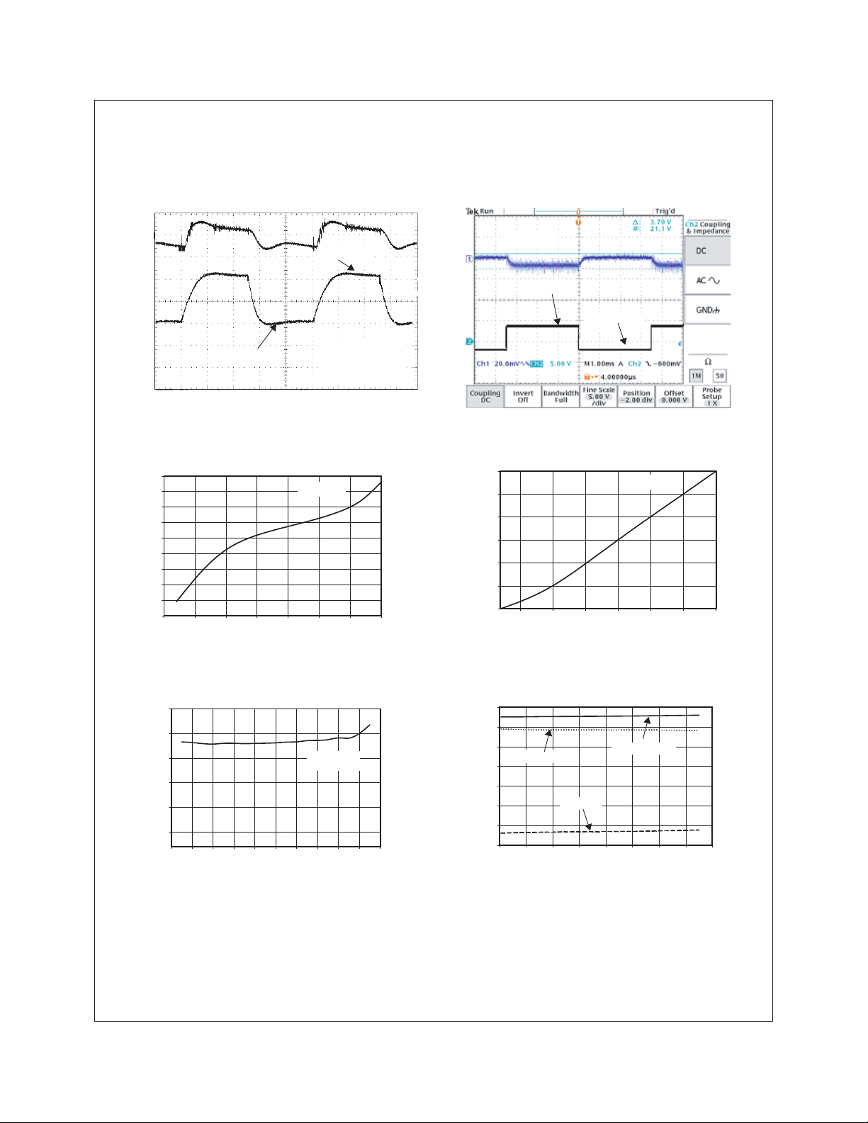
Typical Performance Characteristics
T
= 25°C, C
A
IN
= C
=10µF, C
OUT
= 1µF, V
B
OUT
= 1.3V, unless otherwise noted.
FAN5601 Regulated Step-Down Charge Pump DC/DC Converter
Line Transient Response
(50mV/div)
Output Voltage
VIN = 2V
(1V/div)
Input Voltage
Time (10µs/div)
Input Current vs Input Voltage
46
44
42
A)
µ
40
38
36
34
32
Input Current (
30
28
2.0 2.5 3.0 3.5 4.0 4.5 5.0 5 .5
Input Voltage (V)
I
= 0mA
OUT
VIN = 4.4V
VIN
I
OUT
= 2 V to 4.4V
= 10mA
Load Current
Output Voltage
(20mV/div)
(100mA/div)
Load Transient Response
VIN = 3.3V
I
= 100mA
OUT
I
= 1mA
OUT
Time (1ms/div)
Shutdown Current vs Input Voltage
70
60
50
40
30
20
Shutdown Current (nA)
10
2.5 3.0 3.54.04.55.05.5
Input Voltage (V)
V
= 0V
OUT
Output Voltage vs Ambient Temperature
1.31
1.30
1.29
1.28
1.27
Output Voltage (V)
1.26
-60 -40 -20 0 20 40 60 80 100 120 140
FAN5601 Rev. 1.0.5
V
= 4V
IN
I
= 10mA
OUT
Ambient Temperature (°C)
Mode Change Threshold and Hysteresis
vs Load Current
3.5
3.0
2.5
Low Threshold
2.0
1.5
1.0
0.5
Threshold and Hysteresis (V)
0.0
020406080100120140160
Hysteresis
Load Current (mA)
5
High Threshold
www.fairchildsemi.com
 Loading...