June 2012
FAN53601 / FAN53611
6MHz 600mA / 1A Synchronous Buck Regulator
Features
600mA or 1A Output Current Capability
24µA Typical Quiescent Current
6MHz Fixed-Frequency Operation
Best-in-Class Load Transient Response
Best-in-Class Efficiency
2.3V to 5.5V Input Voltage Range
0.8 to 2V Fixed Output Voltage
Low Ripple Light-Load PFM Mode
Forced PWM and External Clock Synchronization
Internal Soft-Start
Input Under-Voltage Lockout (UVLO)
Thermal Shutdown and Overload Protection
Optional Output Discharge
6-Bump WLCSP, 0.4mm Pitch
Applications
6-Bump WLCSP, 0.4mm Pitch
3G, 4G, WiFi
®
, WiMAX™, and WiBro® Data Cards
Tablets
DSC, DVC
Netbooks
All trademarks are the property of their respective owners.
®
, Ultra-Mobile PCs
Description
The FAN53601/11 is a 6MHz, step-down switching voltage
regulator, available in 600mA or 1A options, that delivers a
fixed output from an input voltage supply of 2.3V to 5.5V.
Using a proprietary architecture with synchronous
rectification, the FAN53601/11 is capable of delivering a
peak efficiency of 92%, while maintaining efficiency over
80% at load currents as low as 1mA.
The regulator operates at a nominal fixed frequency of
6MHz, which reduces the value of the external components
to as low as 470nH for the output inductor and 4.7µF for the
output capacitor. In addition, the Pulse Width Modulation
(PWM) modulator can be synchronized to an external
frequency source.
At moderate and light loads, Pulse Frequency Modulation
(PFM) is used to operate the device in Power-Save Mode
with a typical quiescent current of 24µA. Even with such a
low quiescent current, the part exhibits excellent transient
response during large load swings. At higher loads, the
system automatically switches to fixed-frequency control,
operating at 6MHz. In Shutdown Mode, the supply current
drops below 1µA, reducing power consumption. For
applications that require minimum ripple or fixed frequency,
PFM Mode can be disabled using the MODE pin.
The FAN53601/11 is available in 6-bump, 0.4mm pitch,
Wafer-Level Chip-Scale Package (WLCSP).
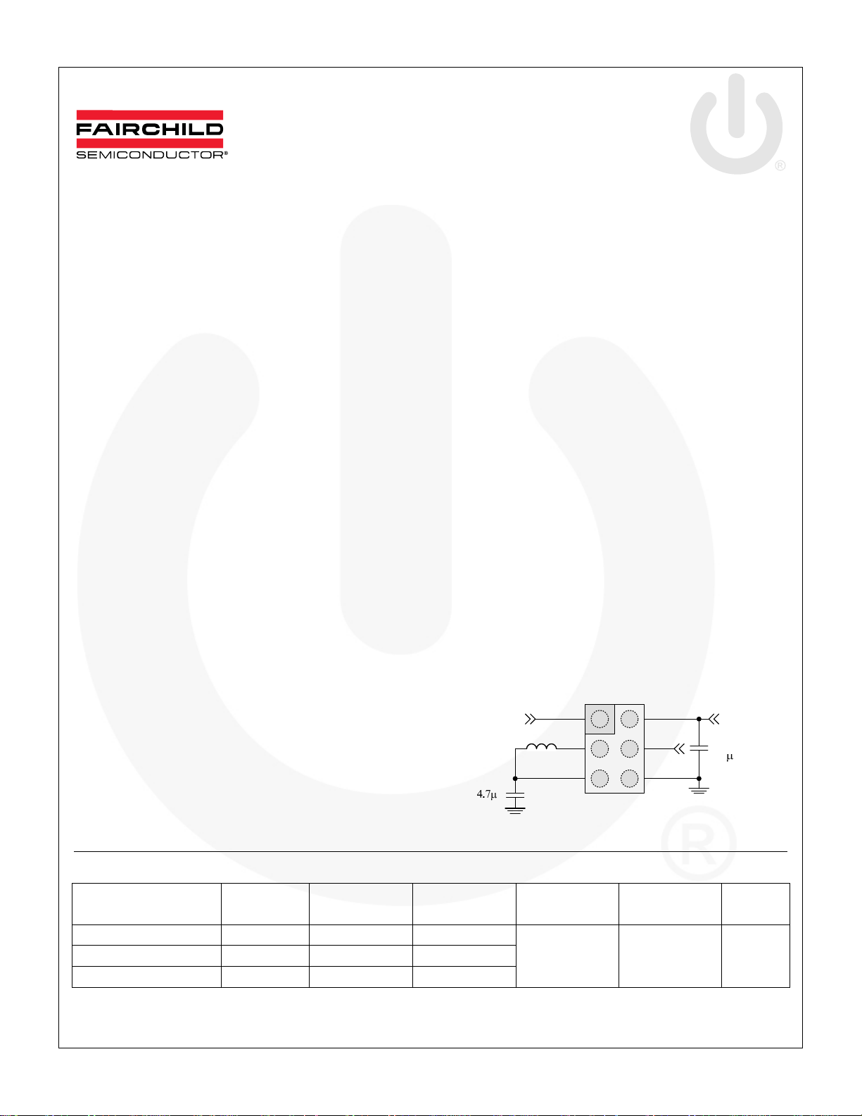
MODE
L1
SW
470nH
FB
C
F
OUT
A1
B1
C1
A2
B2
C2
VIN
EN
GND
C
IN
2.2 F
FAN53601 / FAN53611 — 6MHz, 600mA / 1A Synchronous Buck Regulator
Figure 1. Typical Application
Ordering Information
Part Number
FAN53611AUC11X 1.100V 1A Yes
FAN53611UC123X 1.233V 1A No
FAN53601UC182X 1.820V 600mA No
Notes:
1. Other voltage options available on request. Contact a Fairchild representative.
2. All voltage and output current options are available with or without active discharge. Contact a Fairchild representative.
© 2010 Fairchild Semiconductor Corporation www.fairchildsemi.com
FAN53601 / FAN53611 • Rev. 1.0.0
Output
Voltage
Max. Output
(1)
Current
Active
Discharge
(2)
Package
WLCSP-6,
0.4mm Pitch
Temperature
Range
–40 to +85°C
Packing
Tape and
Reel

Pin Configurations
FAN53601 / FAN53611 — 6MHz, 600mA / 1A Synchronous Buck Regulator
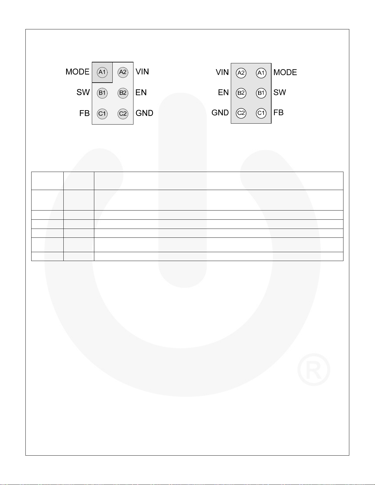
Figure 2. Bumps Facing Down Figure 3. Bumps Facing Up
Pin Definitions
Pin # Name Description
MODE. Logic 1 on this pin forces the IC to stay in PWM Mode. A logic 0 allows the IC to
A1 MODE
B1 SW
C1 FB
C2 GND
B2 EN
A2 VIN
automatically switch to PFM during light loads. The regulator also synchronizes its switching
frequency to four times the frequency provided on this pin. Do not leave this pin floating.
Switching Node. Connect to output inductor.
Feedback / V
Ground. Power and IC ground. All signals are referenced to this pin.
Enable. The device is in Shutdown Mode when voltage to this pin is <0.4V and enabled when >1.2V.
Do not leave this pin floating.
Input Voltage. Connect to input power source.
. Connect to output voltage.
OUT
© 2010 Fairchild Semiconductor Corporation www.fairchildsemi.com
FAN53601 / FAN53611 • Rev. 1.0.0 2

FAN53601 / FAN53611 — 6MHz, 600mA / 1A Synchronous Buck Regulator
Absolute Maximum Ratings
Stresses exceeding the absolute maximum ratings may damage the device. The device may not function or be operable above
the recommended operating conditions and stressing the parts to these levels is not recommended. In addition, extended
exposure to stresses above the recommended operating conditions may affect device reliability. The absolute maximum ratings
are stress ratings only.
Symbol Parameter Min. Max. Units
VIN Input Voltage –0.3 7.0 V
VSW Voltage on SW Pin –0.3 VIN + 0.3
V
EN and MODE Pin Voltage –0.3 VIN + 0.3
CTRL
Other Pins –0.3 VIN + 0.3
ESD
Electrostatic Discharge
Protection Level
Human Body Model per JESD22-A114 3.5
Charged Device Model per JESD22-C101 1.5
TJ Junction Temperature –40 +150 °C
T
Storage Temperature –65 +150 °C
STG
TL Lead Soldering Temperature, 10 Seconds +260 °C
Note:
3. Lesser of 7V or VIN+0.3V.
(3)
(3)
(3)
V
V
V
kV
Recommended Operating Conditions
The Recommended Operating Conditions table defines the conditions for actual device operation. Recommended operating
conditions are specified to ensure optimal performance to the datasheet specifications. Fairchild does not recommend exceeding
them or designing to Absolute Maximum Ratings.
Symbol Parameter Min. Typ. Max. Units
VCC Supply Voltage Range 2.3 5.5 V
I
OUT
L Inductor 470 nH
CIN Input Capacitor 2.2 µF
C
OUT
TA Operating Ambient Temperature –40 +85 °C
TJ Operating Junction Temperature –40 +125 °C
Output Current for FAN53601 0 600 mA
Output Current for FAN53611 0 1 A
Output Capacitor 1.6 4.7 12.0
μF
Thermal Properties
Junction-to-ambient thermal resistance is a function of application and board layout. This data is measured with four-layer 1s2p
boards in accordance to JEDEC standard JESD51. Special attention must be paid to not exceed junction temperature T
given ambient temperate T
.
A
J(max)
at a
Symbol Parameter Typical Unit
JA
© 2010 Fairchild Semiconductor Corporation www.fairchildsemi.com
FAN53601 / FAN53611 • Rev. 1.0.0 3
Junction-to-Ambient Thermal Resistance 150 °C/W

Electrical Characteristics
Minimum and maximum values are at VIN = VEN = 2.3V to 5.5V, V
Figure 1, unless otherwise noted. Typical values are at T
= 25°C, VIN = VEN = 3.6V.
A
Symbol Parameter Conditions Min. Typ. Max. Units
Power Supplies
IQ Quiescent Current
I
Shutdown Supply Current EN = GND 0.25 1.00 µA
(SD)
V
Under-Voltage Lockout Threshold Rising VIN 2.15 2.27 V
UVLO
V
Under-Voltage Lockout Hysteresis 200 mV
UVHYST
Logic Inputs: EN and MODE Pins
VIH Enable HIGH-Level Input Voltage 1.2 V
VIL Enable LOW-Level Input Voltage 0.4 V
V
Logic Input Hysteresis Voltage 100 mV
LHYST
IIN Enable Input Leakage Current Pin to VIN or GND 0.01 1.00 µA
Switching and Synchronization
fSW Switching Frequency
f
MODE Synchronization Range
SYNC
(4)
V
Regulation
1.233V
Output Voltage
VO
Accuracy
1.820V
tSS Soft-Start From EN Rising Edge 180 300 µs
Output Driver
No load, Not Switching 24 50 µA
PWM Mode 8 mA
= 3.6V, TA = 25°C 5.4 6.0 6.6 MHz
IN
(4)
Square Wave at MODE Input 1.3 1.5 1.7 MHz
= 0 to 1A 1.207 1.233 1.272 V
I
LOAD
PWM Mode 1.207 1.233 1.259 V
= 0 to 1A 1.784 1.820 1.875 V
I
LOAD
PWM Mode 1.784 1.820 1.856 V
= 0V (AUTO Mode), TA = -40°C to +85°C; circuit of
MODE
FAN53601 / FAN53611 — 6MHz, 600mA / 1A Synchronous Buck Regulator
R
DS(on)
PMOS On Resistance V
NMOS On Resistance VIN = VGS = 3.6V 165
= VGS = 3.6V 175
IN
m
m
Open-Loop for FAN53601 900 1100 1250 mA
I
PMOS Peak Current Limit
LIM(OL)
R
Output Discharge Resistance EN = GND 230
DIS
T
Thermal Shutdown 150 °C
TSD
T
Thermal Shutdown Hysteresis 15 °C
HYS
Open-Loop for FAN53611 1500 1750 2000 mA
Notes:
4. Limited by the effect of t
minimum (see Operation Description section).
OFF
5. The Electrical Characteristics table reflects open-loop data. Refer to the Operation Description and Typical Characteristics
Sections for closed-loop data.
© 2010 Fairchild Semiconductor Corporation www.fairchildsemi.com
FAN53601 / FAN53611 • Rev. 1.0.0 4

Typical Performance Characteristics
Unless otherwise noted, VIN = VEN = 3.6V, V
= 0V (AUTO Mode), V
MODE
= 1.82V, and TA = 25°C.
OUT
FAN53601 / FAN53611 — 6MHz, 600mA / 1A Synchronous Buck Regulator
95%
90%
85%
Effici ency
80%
75%
70%
0 200 400 600 800 1000
Load Cu rrent (mA)
2.7 VIN
3.6 VIN
4.2 VIN
5.0 VIN
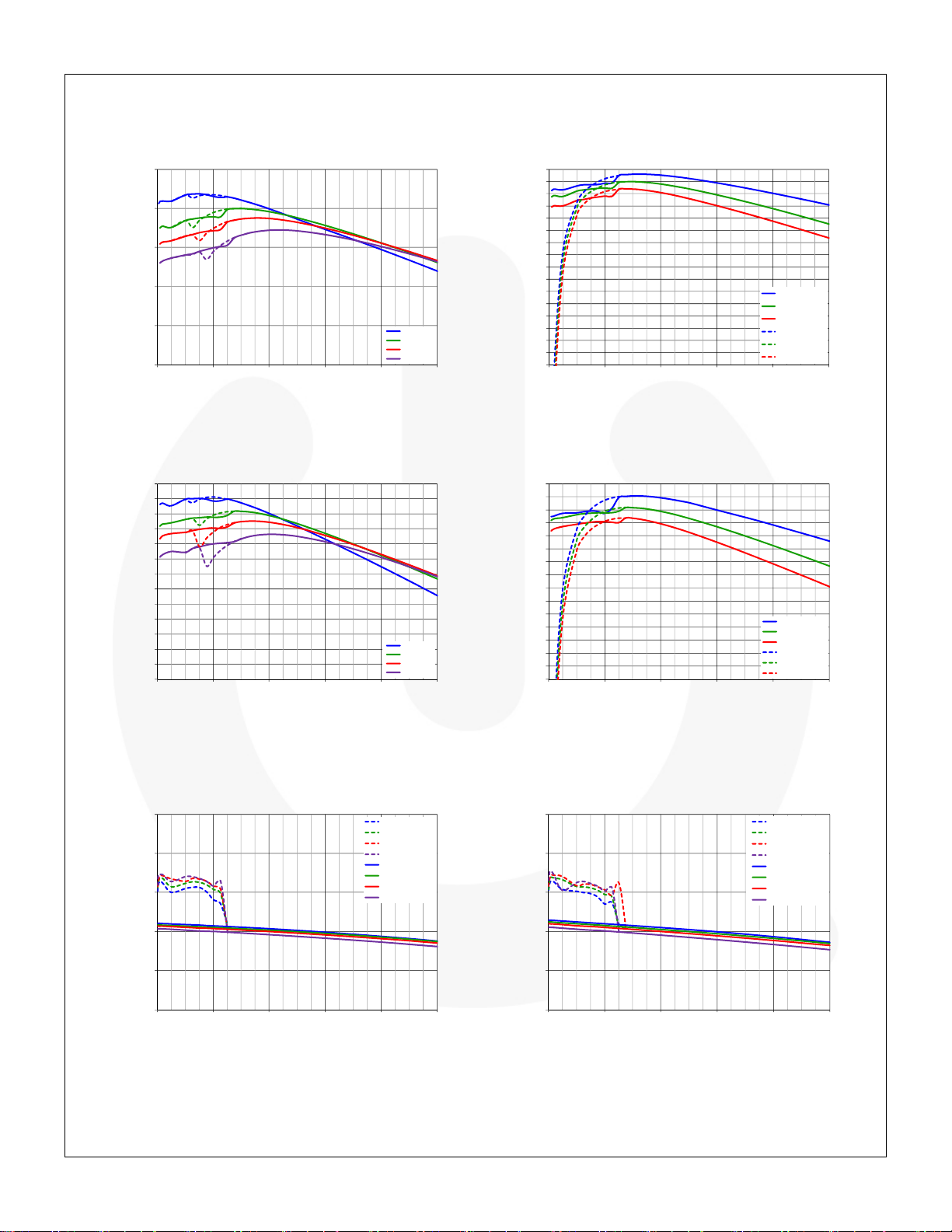
Figure 4. Efficiency vs. Load Current and
Input Voltage, Auto Mode, Dotted for Decreasing Load
90%
88%
86%
84%
82%
80%
78%
76%
Effici ency
74%
72%
70%
68%
66%
64%
0 200 400 600 800 1000
Load Cu rrent (mA)
2.7 VIN
3.6 VIN
4.2 VIN
5.0 VIN
Figure 6. Efficiency vs. Load Current and
Input Voltage, V
= 1.23V, Auto Mode, Dotted for
OUT
Decreasing Load
92%
90%
88%
86%
84%
82%
80%
78%
76%
74%
Effici ency
72%
70%
68%
66%
64%
62%
60%
and Temperature, Auto Mode, Dotted for FPWM
90%
88%
86%
84%
82%
80%
78%
76%
74%
Effici ency
72%
70%
68%
66%
64%
62%
60%
and Temperature, V
- 40C, AUTO
+25C, AUTO
+85C, AUTO
- 40C, PWM
+25C, PWM
+85C, PWM
0 200 400 600 800 1000
Load Cu rrent (mA)
Figure 5. Efficiency vs. Load Current
-40C, AUTO
+25C, AUT O
+85C, AUT O
-40C, PWM
+25C, PW M
+85C, PW M
0 200 400 60 0 800 1000
Load Current (mA)
Figure 7. Efficiency vs. Load Current
=1.23V, Auto Mode, Dotted for
OUT
FPWM
3
2
1
0
Output Regulation (%)
-1
-2
0 200 400 600 800 1000
Figure 8. ∆V
(%) vs. Load Current and Input Voltage,
OUT
Normalized to 3.6V
2.7VIN, AUTO
3.6VIN, AUTO
4.2VIN, AUTO
5.0VIN, AUTO
2.7VIN, PWM
3.6VIN, PWM
4.2VIN, PWM
5.0VIN, PWM
Load Current (mA)
, 500mA Load, FPWM, Dotted for
IN
Auto Mode
Figure 9. ∆V
3
2
1
0
Output Regulation (%)
-1
-2
0 200 400 600 800 1000
Load Current (mA)
(%) vs. Load Current and Input Voltage,
V
=1.23V, Normalized to 3.6VIN, 500mA Load, FPWM,
OUT
OUT
2.7VIN, AUTO
3.6VIN, AUTO
4.2VIN, AUTO
5.0VIN, AUTO
2.7VIN, PWM
3.6VIN, PWM
4.2VIN, PWM
5.0VIN, PWM
Dotted for Auto Mode
© 2010 Fairchild Semiconductor Corporation www.fairchildsemi.com
FAN53601 / FAN53611 • Rev. 1.0.0 5
 Loading...