Fairchild FAN5355 service manual

November 2011
FAN5355
1.1A / 1A / 0.8A, 3MHz Digitally Programmable Regulator
Features
93% Efficiency at 3MHz
800mA, 1A, or 1.1A Output Current
2
I
C™-Compatible Interface up to 3.4Mbps
6-bit V
Programmable from 0.75V to 1.975V
OUT
2.7V to 5.5V Input Voltage Range
3MHz Fixed-Frequency Operation
Excellent Load and Line Transient Response
Small Size, 1H Inductor Solution
±2% PWM DC Voltage Accuracy
35ns Minimum On-Time
High-Efficiency, Low-Ripple, Light-Load PFM
Smooth Transition between PWM and PFM
37A Operating PFM Quiescent Current
Pin-Selectable or I
2C™
Programmable Output Voltage
On-the-Fly External Clock Synchronization
10-lead MLP (3 x 3mm) or 12-bump CSP Packages
Applications
Cell Phones, Smart Phones
3G, WiFi
Netbooks
®
, WiMAX™, and WiBro® Data Cards
®
, Ultra-Mobile PCs
SmartReflex™-Compliant Power Supply
Split Supply DSPs and P Solutions OMAP™, XSCALE™
Mobile Graphic Processors (NVIDIA
®
, ATI)
LPDDR2 and Memory Modules
Description
The FAN5355 device is a high-frequency, ultra-fast transient
response, synchronous step-down DC-DC converter
optimized for low-power applications using small, low-cost
inductors and capacitors. The FAN5355 supports up to
800mA, 1A, or 1.1A load current.
The device is ideal for mobile phones and similar portable
applications powered by a single-cell Lithium-Ion battery. With
an output-voltage range adjustable via I
0.75V to 1.975V, the device supports low-voltage DSPs and
processors, core power supplies, and memory modules in
smart phones, PDAs, and handheld computers.
The FAN5355 operates at 3MHz (nominal) fixed switching
frequency using either its internal oscillator or an external
SYNC frequency.
During light-load conditions, the regulator includes a PFM
mode to enhance light-load efficiency. The regulator
transitions smoothly between PWM and PFM modes with no
glitches on V
consumption is reduced to less than 200nA.
The serial interface is compatible with Fast/Standard and
High-Speed mode I
3.4Mbps. This interface is used for dynamic voltage scaling
with 12.5mV voltage steps for reprogramming the mode of
operation (PFM or Forced PWM), or to disable/enable the
output voltage.
The chip's advanced protection features include short-circuit
protection and current and temperature limits. During a
sustained over-current event, the IC shuts down and restarts
after a delay to reduce average power dissipation into a fault.
During startup, the IC controls the output slew rate to minimize
input current and output overshoot at the end of soft start. The
IC maintains a consistent soft-start ramp, regardless of output
load during startup.
The FAN5355 is available in 10-lead MLP (3x3mm) and
12-bump WLCSP packages.
. In hardware shutdown, the current
OUT
2
C specifications, allowing transfers up to
2
C™ interface from
FAN5355 — 1.1A / 1A / 0.8A, 3MHz Digitally Programmable Regulator
All trademarks are the property of th eir resp ecti ve owner s.
© 2008 Fairchild Semiconductor Corporation www.fairchildsemi.com
FAN5355 • Rev. 1.1.0
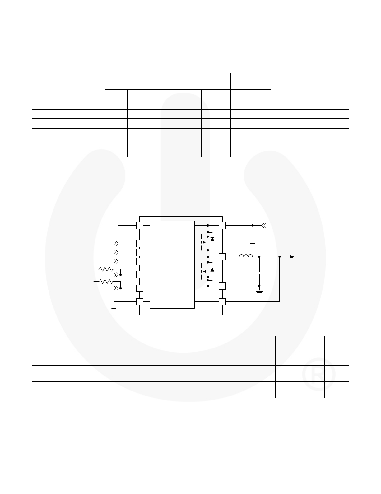
Ordering Information
FAN5355 — 1.1A / 1A / 0.8A, 3MHz Digitally Programmable Regulator
Order Number
(1)
Option
Slave Address
LSB
A1 A0 mA Min. Max. VSEL0 VSEL1
Output
Current V
Programming
OUT
Power-up
Defaults
Package
FAN5355UC00X 00 0 0 800 0.7500 1.5375 1.05 1.35 WLCSP-12, 2.23x1.46mm
FAN5355MP00X 00 0 0 800 0.7500 1.5375 1.05 1.35 MLP-10, 3x3mm
FAN5355UC02X
02 1 0 800
0.7500
1.4375
(2)
1.05 1.20
WLCSP-12, 2.23x1.46mm
FAN5355UC03X 03 0 0 1000 0.7500 1.5375 1.00 1.20 WLCSP-12, 2.23x1.46mm
FAN5355UC06X 06 0 0 1000 1.1875 1.9750 1.80 1.80 WLCSP-12, 2.23x1.46mm
FAN5355UC08X
08 1 0 1100
0.7500
1.4375
(2)
1.05 1.20
WLCSP-12, 2.23x1.46mm
Notes:
1. The “X” designator specifies tape and reel packaging.
2. V
is limited to the maximum voltage for all VSEL codes greater than the maximum V
OUT
OUT
listed.
Typical Application
AVIN
Q1
EN
VSEL
SYNC
Q2
MODULATOR
SDA
VCCIO
SCL
PVIN
SW
PGND
VIN
C
IN
VOUT
L
OUT
C
OUT
AGND
VOUT
Figure 1. Typical Application
Component Description Vendor Parameter Min. Typ. Max. Units
(3)
L
L1 (L
C
CIN
OUT
OUT
)
1H nominal
0603
6x0.8x0.8)
(1.
10F X5R or better
0603 (1.6x0.8x0.8)
4.7F X5R or better
Murata LQM31P
or FDK MIPSA2520
Murata or equivalent
GRM188R60G106ME47D
Murata or equivalent
GRM188R60J475KE19D
DCR (series R) 100
0.7 1.0 1.2
(4)
C
5.6 10.0 12.0
(4)
C
3.0 4.7 5.6
Table 1. Recommended External Components
Notes:
3. Minimum L incorporates tolerance, temperature, and partial saturation effects (L decreases with increasing current).
4. Minimum C is a function of initial tolerance, maximum temperature, and the effective capacitance being reduced due to
frequency, dielectric, and voltage bias effects.
© 2008 Fairchild Semiconductor Corporation 2 www.fairchildsemi.com
FAN5355 • Rev. 1.1.0
H
m
F
F
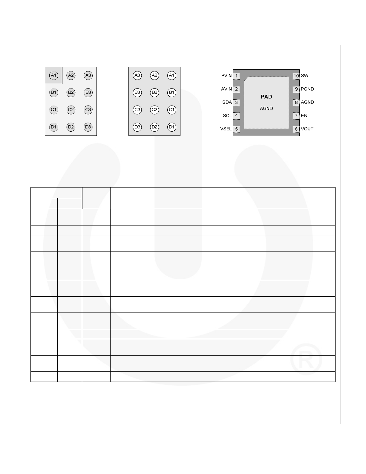
Pin Configuration
FAN5355 — 1.1A / 1A / 0.8A, 3MHz Digitally Programmable Regulator
Top View
Bottom View
Top View
Figure 2. WLCSP-12, 2.23x1.46mm Figure 3. MLP10, 3x3mm
Pin Definitions
Pin #
WLCSP MLP
A1, B1 9 PGND
A2 10 SW
A3 1 PVIN
B2 N/A SYNC
B3 2 AVIN
C1 8, PAD AGND
C2 7 EN
C3 3 SDA
D1 6 VOUT
D2 5 VSEL
D3 4 SCL
Note:
5. All logic inputs (SDA, SCL, SYNC, EN, and VSEL) are high impedance and should not be left floating. For minimum
quiescent power consumption, tie unused logic inputs to AVIN or AGND. If I
Name
(5)
Description
Power GND. Power return for gate drive and power transistors. Connect to AGND on PCB.
The connection from this pin to the bottom of C
should be as short as possible.
IN
Switching Node. Connect to output inductor.
Power Input Voltage. Connect to input power source. The connection from this pin to CIN
should be as short as possible.
Sync. When toggling and SYNC_EN bit is HIGH, the regulator synchronizes to the frequency
on this pin. In PWM mode, when this pin is statically LOW or statically HIGH, or when its
frequency is outside of the specified capture range, the regulator’s frequency is controlled by
its internal 3MHz clock.
Analog Input Voltage. Connect to input power source as close as possible to the input
bypass capacitor.
Analog GND. This is the signal ground reference for the IC. All voltage levels are measured
with respect to this pin.
Enable. When this pin is HIGH, the circuit is enabled. When LOW, quiescent current is
minimized. This pin should not be left floating.
2
SDA. I
C interface serial data.
Output Voltage Monitor. Tie this pin to the output voltage. This is a signal input pin to the
control circuit and does not carry DC current.
Voltage Select. When HIGH, V
behavior can be overridden through I
2
SCL. I
C interface serial clock.
is set by VSEL1. When LOW, V
OUT
2
C register settings. This pin should not be left floating.
2
C control is unused, tie SDA and SCL to AVIN.
is set by VSEL0. This
OUT
© 2008 Fairchild Semiconductor Corporation 3 www.fairchildsemi.com
FAN5355 • Rev. 1.1.0
Absolute Maximum Ratings
Stresses exceeding the absolute maximum ratings may damage the device. The device may not function or be operable above
the recommended operating conditions and stressing the parts to these levels is not recommended. In addition, extended
exposure to stresses above the recommended operating conditions may affect device reliability. The absolute maximum ratings
are stress ratings only.
Symbol Parameter Min. Max. Unit
VCC
ESD
TJ Junction Temperature –40 +150 °C
T
STG
TL Lead Soldering Temperature, 10 Seconds +260 °C
Note:
6. Lesser of 6.5V or AVIN+0.3V.
AVIN, SW, PVIN Pins -0.3 6.5 V
Other Pins -0.3 AVIN + 0.3
Electrostatic Discharge
Protection Level
Human Body Model per JESD22-A114 3.5 KV
Charged Device Model per JESD22-C101 1.5 KV
(6)
V
Storage Temperature –65 +150 °C
Recommended Operating Conditions
The Recommended Operating Conditions table defines the conditions for actual device operation. Recommended operating
conditions are specified to ensure optimal performance to the datasheet specifications. Fairchild does not recommend exceeding
them or designing to absolute maximum ratings.
FAN5355 — 1.1A / 1A / 0.8A, 3MHz Digitally Programmable Regulator
Symbol Parameter Min. Max. Unit
VIN Supply Voltage 2.7 5.5 V
f Frequency Range 2.7 3.3 MHz
V
SDA and SCL Voltage Swing
CCIO
(7)
2.5 V
TA Ambient Temperature –40 +85 °C
TJ Junction Temperature –40 +125 °C
Note:
2
7. The I
C interface operates with t
swings greater than 2.5V are required (for example if the I
increased to 80ns. Most I
provides ample t
HD;DAT
2
C masters change SDA near the midpoint between the falling and rising edges of SCL, which
.
= 0 as long as the pull-up voltage for SDA and SCL is less than 2.5V. If voltage
HD;DAT
2
C bus is pulled up to VIN), the minimum t
HD;DAT
must be
Dissipation Ratings
Package
Molded Leadless Package (MLP) 49ºC/W 2050mW 21mW/ºC
Wafer-Level Chip-Scale Package (WLCSP) 110ºC/W 900mW 9mW/ºC
Notes:
8. Maximum power dissipation is a function of T
allowable ambient temperature is P
9. This thermal data is measured with high-K board (four-layer board according to JESD51-7 JEDEC standard).
(8)
(9)
θ
= [T
D
J(max)
J(max)
JA
Power Rating at T
, θJA, and TA. The maximum allowable power dissipation at any
- TA ] / θJA.
≤ 25°C Derating Factor > TA = 25ºC
A
© 2008 Fairchild Semiconductor Corporation 4 www.fairchildsemi.com
FAN5355 • Rev. 1.1.0
Electrical Specifications
VIN = 3.6V, EN = VIN, VSEL = VIN, SYNC = GND, VSEL0(6) bit = 1, CONTROL2[4:3] = 00. TA = -40°C to +85°C, unless otherwise
noted. Typical values are at T
Symbol Parameter Conditions Min. Typ. Max. Units
Power Supplies
VIN Input Voltage Range 2.7 5.5 V
IQ Quiescent Current
ISD Shutdown Supply Current
V
Under-Voltage Lockout Threshold
UVLO
V
ENABLE, VSEL, SDA, SCL, SYNC
Power Switch and Protection
R
R
Frequency Control
Under-Voltage Lockout Hysteresis 200 250 300 mV
UVHYST
VIH HIGH-Level Input Voltage 1.2 V
VIL LOW-Level Input Voltage 0.4 V
IIN Input Bias Current Input tied to GND or VIN 0.01 1.00
DS(ON)P
I
LKGP
DS(ON)N
I
LKGN
R
I
LIMPK
T
LIMIT
T
HYST
Resistance
P-Channel Leakage Current VDS = 6V 1
N-Channel MOSFET On
Resistance
N-Channel Leakage Current VDS = 6V 1
Discharge Resistor for Power-
DIS
Down Sequence
P-MOS Current Limit
Thermal Shutdown 150 °C
Thermal Shutdown Hysteresis 20 °C
P-Channel MOSFET On
fSW Oscillator Frequency 2.65 3.00 3.35 MHz
f
Synchronization Range 2.7 3.0 3.3 MHz
SYNC
D
Synchronization Duty Cycle 20 80 %
SYNC
= 25°C. Circuit and components according to Figure 1.
A
IO = 0mA, PFM Mode 37 50
IO = 0mA, 3MHz PWM Mode 4.8 mA
EN = GND 0.1 2.0
EN = VIN, EN_DCDC bit = 0,
SDA = SCL = V
V
Rising 2.40 2.60 V
IN
IN
VIN Falling 2.00 2.15 2.30 V
V
= 3.6V, CSP Package 145
IN
VIN = 3.6V, MLP Package 165
VIN = 2.7V, MLP Package 200
V
= 3.6V, CSP Package 75
IN
VIN = 3.6V, MLP Package 95
VIN = 2.7V, MLP Package 101
Options 03 and 06 60 120 Ω
2.7V ≤ V
≤ 4.2V, Options 00 and 02 1150 1350 1600
IN
2.7V ≤ VIN ≤ 5.5V, Options 00 and 02 1050 1350 1600
2.7V ≤ VIN ≤ 4.2V, Options 03 and 06 1350 1550 1800
2.7V ≤ VIN ≤ 5.5V, Options 03 and 06 1250 1550 1800
2.7V ≤ VIN ≤ 4.5V, Option 08 1400 1650
0.1 2.0
Continued on the following page…
A
A
A
mΩ
A
mΩ
A
mA
FAN5355 — 1.1A / 1A / 0.8A, 3MHz Digitally Programmable Regulator
© 2008 Fairchild Semiconductor Corporation 5 www.fairchildsemi.com
FAN5355 • Rev. 1.1.0

Electrical Specifications (Continued)
= 3.6V, EN = VIN, VSEL = VIN, SYNC = GND, VSEL0(6) bit = 1, CONTROL2[4:3] = 00. TA = -40°C to +85°C, unless otherwise
V
IN
noted. Typical values are at T
Symbol Parameter Conditions Min. Typ. Max. Units
Output Regulation
= 25°C. Circuit and components according to Figure 1.
A
I
= 0, Forced PWM, V
OUT(DC)
= 1.35V –1.5 1.5 %
OUT
FAN5355 — 1.1A / 1A / 0.8A, 3MHz Digitally Programmable Regulator
V
OUT
V
OUT
Accuracy
Option 00
Option 02
Option 03
Option 06
2.7V ≤ VIN ≤ 5.5V, V
= 0 to 800mA, Forced PWM
I
OUT(DC)
2.7V ≤ VIN ≤ 5.5V, V
= 0 to 800mA, PFM Mode
I
OUT(DC)
= 0, Forced PWM, V
I
OUT(DC)
2.7V ≤ VIN ≤ 5.5V, V
= 0 to 800mA, Forced PWM
I
OUT(DC)
2.7V ≤ VIN ≤ 5.5V, V
= 0 to 800mA, PFM Mode
I
OUT(DC)
= 0, Forced PWM, V
I
OUT(DC)
2.7V ≤ VIN ≤ 5.5V, V
= 0 to 1A, Forced PWM
I
OUT(DC)
2.7V ≤ VIN ≤ 5.5V, V
= 0 to 1A, PFM Mode
I
OUT(DC)
= 0, Forced PWM, V
I
OUT(DC)
2.7V ≤ VIN ≤ 5.5V, V
= 0 to 1A, Forced PWM
I
OUT(DC)
2.7V ≤ VIN ≤ 5.5V, V
= 0 to 1A, PFM Mode
I
OUT(DC)
OUT
OUT
OUT
OUT
OUT
OUT
OUT
OUT
from 0.75 to 1.5375,
from 0.75 to 1.5375,
= 1.20V –1.5 1.5 %
OUT
from 0.75 to 1.4375,
from 0.75 to 1.4375,
= 1.20V –1.5 1.5 %
OUT
from 0.75 to 1.5375,
from 0.75 to 1.5375,
= 1.800V –1.5 1.5 %
OUT
from 1.185 to 1.975,
from 1.185 to 1.975,
–2 2 %
–1.5 3.5 %
–2 2 %
–1.5 3.5 %
–2 2 %
–1.5 3.5 %
–2 2 %
–1.5 3.5 %
= 0, Forced PWM, V
I
OUT(DC)
Option 08
2.7V ≤ VIN ≤ 5.5V, V
= 0 to 1100mA, Forced PWM
I
OUT(DC)
2.7V ≤ VIN ≤ 5.5V, V
= 0 to 1100mA, PFM Mode
I
OUT(DC)
OUT
IV
LOAD
VV
V
RIPPLE
© 2008 Fairchild Semiconductor Corporation 6 www.fairchildsemi.com
FAN5355 • Rev. 1.1.0
Load Regulation I
OUT
Line Regulation 2.7V ≤ V
IN
Output Ripple Voltage
= 0 to 800mA, Forced PWM –0.5 %/A
OUT(DC)
≤ 5.5V, I
IN
PWM Mode, V
PFM Mode, I
OUT
OUT(DC)
from 0.75 to 1.4375,
OUT
from 0.75 to 1.4375,
OUT
OUT(DC)
= 1.35V 2.2 mVPP
= 10mA 20 mVPP
= 1.20V –1.5 1.5 %
OUT
–2 2 %
–1.5 3.5 %
= 300mA 0 %/V
Continued on the following page…
Electrical Specifications (Continued)
= 3.6V, EN = VIN, VSEL = VIN, SYNC = GND, VSEL0(6) bit = 1, CONTROL2[4:3] = 00. TA = -40°C to +85°C, unless otherwise
V
IN
noted. Typical values are at T
Symbol Parameter Conditions Min. Typ. Max. Units
6-Bit DAC
Differential Nonlinearity Monotonicity Assured by Design 0.8 LSB
Timing
I2CEN EN HIGH to I2C Start 250
t
V
V(L-H)
Soft Start
tSS
V
Soft-start V
SLEW
Note:
10. Option 03 and 06 slew rates are 35.5V/ms during the first 16s of soft start.
LOW to HIGH Settling
OUT
Regulator
Enable to
Regulated V
= 25°C. Circuit and components according to Figure 1.
A
R
= 75, Transition from 1.0 to
LOAD
1.5375V,
V
Settled to within 2% of Set Point
OUT
OUT
Slew Rate
OUT
Option 06
All Other
Options
(10)
R
R
LOAD
LOAD
> 5, to V
> 5, to V
= 1.8000V
OUT
= Power-up Default
OUT
18.75 V/ms
7
170 210
140 180
s
s
s
s
FAN5355 — 1.1A / 1A / 0.8A, 3MHz Digitally Programmable Regulator
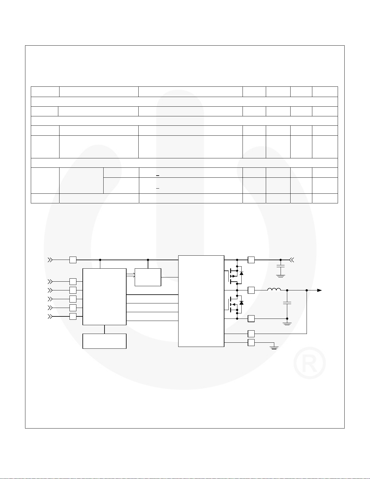
AVIN
EN
VSEL
SYNC
SDA
SCL
I2C
INTERFACE
AND LOGIC
3 MHz Osc
7-bit
DAC
SOFT START
FPWM
EN_REG
Q1
REF
Q2
MODULATOR
CLK
PVIN
SW
PGND
VOUT
AGND
VIN
C
IN
VOUT
L
OUT
C
OUT
Figure 4. Block Diagram
© 2008 Fairchild Semiconductor Corporation 7 www.fairchildsemi.com
FAN5355 • Rev. 1.1.0
I2C Timing Specifications
Guaranteed by design.
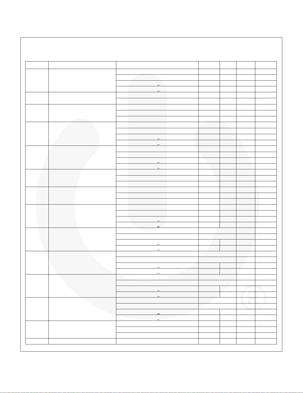
Symbol Parameter Conditions Min. Typ. Max. Units
Standard Mode 100 kHz
f
SCL Clock Frequency
SCL
t
t
HD;STA
t
LOW
t
HIGH
t
SU;STA
t
SU;DAT
t
HD;DAT
t
t
t
RDA
t
RCL1
t
t
SU;STO
Bus-Free Time between STOP and
BUF
START Conditions
START or Repeated-START Hold
Time
SCL LOW Period
SCL HIGH Period
Repeated-START Setup Time
Data Setup Time
Data Hold Time
SCL Rise Time
RCL
SCL Fall Time
FCL
(7)
SDA Rise Time
Rise Time of SCL After a Repeated
START Condition and After ACK Bit
SDA Fall Time
FDA
Stop Condition Setup Time
CB Capacitive Load for SDA and SCL 400 pF
Fast Mode 400 kHz
High-Speed Mode, CB < 100pF 3400 kHz
High-Speed Mode, CB < 400pF 1700 kHz
Standard Mode 4.7
Fast Mode 1.3
Standard Mode 4
s
s
s
Fast Mode 600 ns
High-Speed Mode 160 ns
Standard Mode 4.7
Fast Mode 1.3
s
s
High-Speed Mode, CB < 100pF 160 ns
High-Speed Mode, CB < 400pF 320 ns
Standard Mode 4
s
Fast Mode 600 ns
High-Speed Mode, CB < 100pF 60 ns
High-Speed Mode, CB < 400pF 120 ns
Standard Mode 4.7
s
Fast Mode 600 ns
High-Speed Mode 160 ns
Standard Mode 250 ns
Fast Mode 100 ns
High-Speed Mode 10 ns
Standard Mode 0 3.45
s
Fast Mode 0 900 ns
High-Speed Mode, CB < 100pF 0 70 ns
High-Speed Mode, CB < 400pF 0 150 ns
Standard Mode 20+0.1C
1000 ns
B
Fast Mode 20+0.1CB 300 ns
High-Speed Mode, CB < 100pF 10 80 ns
High-Speed Mode, CB < 400pF 20 160 ns
Standard Mode 20+0.1C
300 ns
B
Fast Mode 20+0.1CB 300 ns
High-Speed Mode, CB < 100pF 10 40 ns
High-Speed Mode, CB < 400pF 20 80 ns
Standard Mode 20+0.1C
1000 ns
B
Fast Mode 20+0.1CB 300 ns
High-Speed Mode, CB < 100pF 10 80 ns
High-Speed Mode, CB < 400pF 20 160 ns
Standard Mode 20+0.1C
300 ns
B
Fast Mode 20+0.1CB 300 ns
High-Speed Mode, CB < 100pF 10 80 ns
High-Speed Mode, CB < 400pF 20 160 ns
Standard Mode 4
s
Fast Mode 600 ns
High-Speed Mode 160 ns
FAN5355 — 1.1A / 1A / 0.8A, 3MHz Digitally Programmable Regulator
© 2008 Fairchild Semiconductor Corporation 8 www.fairchildsemi.com
FAN5355 • Rev. 1.1.0
 Loading...