Fairchild FAN53540 service manual
February 2012
FAN53540
2.4MHz, 5A TinyBuck™ Synchronous Buck Regulator
FAN53540 — 2.4MHz, 5A TinyBuck™ Synchronous Buck Regulator
Features
2.4MHz Fixed-Frequency Operation
Best-in-Class Load Transient Response
5A Output Current Capability
2.7V to 5.5V Input Voltage Range
Adjustable Output Voltage: 0.8V to V
IN
•0.9
PFM Mode for High Efficiency in Light Load
(Forced PWM Available on MODE Pin)
50µA Typical Quiescent Current in PFM Mode
External Frequency Synchronization
Low Ripple Light-Load PFM Mode with Forced
PWM Control
Power Good Output
Internal Soft-Start
Input Under-Voltage Lockout (UVLO)
Thermal Shutdown and Overload Protection
No External Compensation Required
20-Bump WLCSP
Applications
Set-Top Box
Hard Disk Drive
Communications Cards
DSP Power
Description
The FAN53540 is a step-down switching voltage regulator
that delivers an adjustable output from an input voltage
supply of 2.7V to 5.5V. Using a proprietary architecture with
synchronous rectification, the FAN53540 is capable of
delivering 5A at over 90% efficiency, while maintaining a
very high efficiency of over 80% at load currents as low as
2mA. The regulator operates at a nominal fixed frequency of
2.4MHz, which reduces the value of the external
components to 470nH for the output inductor and 20µF for
the output capacitor. Additional output capacitance can be
added to improve regulation during load transients without
affecting stability and inductance up to 1.2µH may be used
with additional output capacitance.
At moderate and light loads, pulse frequency modulation
(PFM) is used to operate the device in power-save mode
with a typical quiescent current of 50µA. Even with such a
low quiescent current, the part exhibits excellent transient
response during large load swings. At higher loads, the
system automatically switches to fixed-frequency control,
operating at 2.4MHz. In shutdown mode, the supply current
drops below 1µA, reducing power consumption. PFM mode
can be disabled if constant frequency is desired. The
FAN53540 is available in a 20-bump 1.96mm x 1.56mm
Wafer-Level Chip-Scale Package (WLCSP).
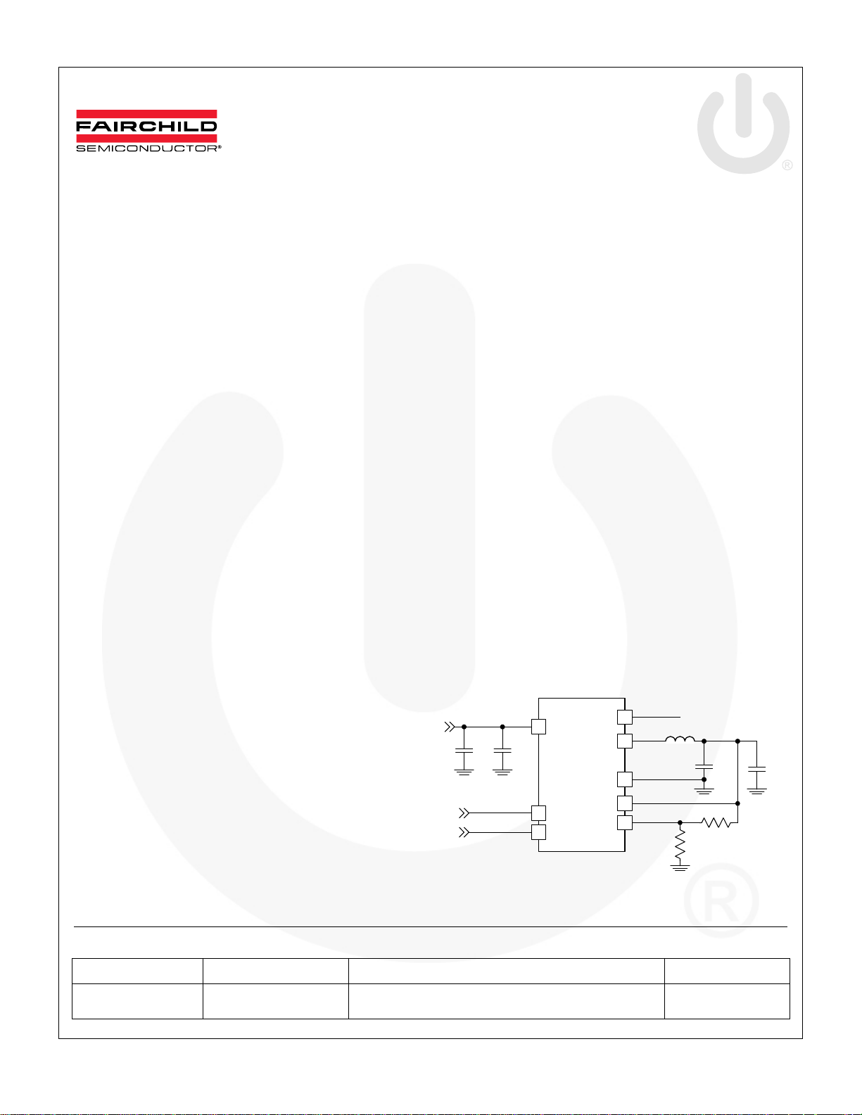
PGOOD
SW
0.47H
GND
VOUT
FB
L1
R2
C
OUT
10F
R1
C
OUT
10F
C
IN
10F
VIN
C
10nF
EN
MODE
IN1
FAN54540
Figure 1. Typical Application
Ordering Information
Part Number Temperature Range Package Packing Method
FAN53540UCX -40 to 85°C
© 2011 Fairchild Semiconductor Corporation www.fairchildsemi.com
FAN53540 • Rev. 1.0.2
20-Ball Wafer-Level, Chip-Scale Package (WLCSP),
4x5 Array, 0.4mm Pitch, 250µm Ball
Tape and Reel
FAN53540 — 2.4 MHz, 5A TinyBuck™ Synchronous Buck Regulator
Recommended External Components
Table 1. Recommended External Components for 5A Maximum Load Current
Component Description Vendor Parameter Typical Unit
L1 470nH Nominal
C
OUT
CIN
C
10nF, 25V, X7R, 0402 Any C 10 nF
IN1
10F, 6.3V, X5R, 0805, 2 Pieces
10F, 6.3V, X5R, 0805
GRM21BR60J106M (Murata)
See Table 2
C2012X5R0J106M (TDK)
L
C 10
0.47
H
F
Table 2. Recommended Inductors
Component Dimensions
Manufacturer Part# L (nH) DCR (mΩ)I
Bourns SRP5012-R47M 470 19 6.0 5.1 4.5 1.2
Bourns SRP4012-R47M 470 20 5.5 4.6 4.0 1.2
Coilcraft XPL4020-471ML 470 19 7.2 4.2 4.2 2.0
Inter-Technical
TDK VLC5020T-R47M 470 15 5.4 5.0 5.0 2.0
Vishay IHLP1616ABERR47M01 470 20 5.0 4.5 4.1 1.2
Notes:
1. I
MAXDC
2. Inductor used for efficiency and temperature rise measurements.
(2)
SC2511-R47M 470 2.6 16.0 6.5 6.5 3.0
is the lesser current to produce 40oC temperature rise or 30% inductance roll-off.
MAXDC
(1)
L W H
© 2011 Fairchild Semiconductor Corporation www.fairchildsemi.com
FAN53540 • Rev. 1.0.2 2
Pin Configuration
FAN53540 — 2.4 MHz, 5A TinyBuck™ Synchronous Buck Regulator
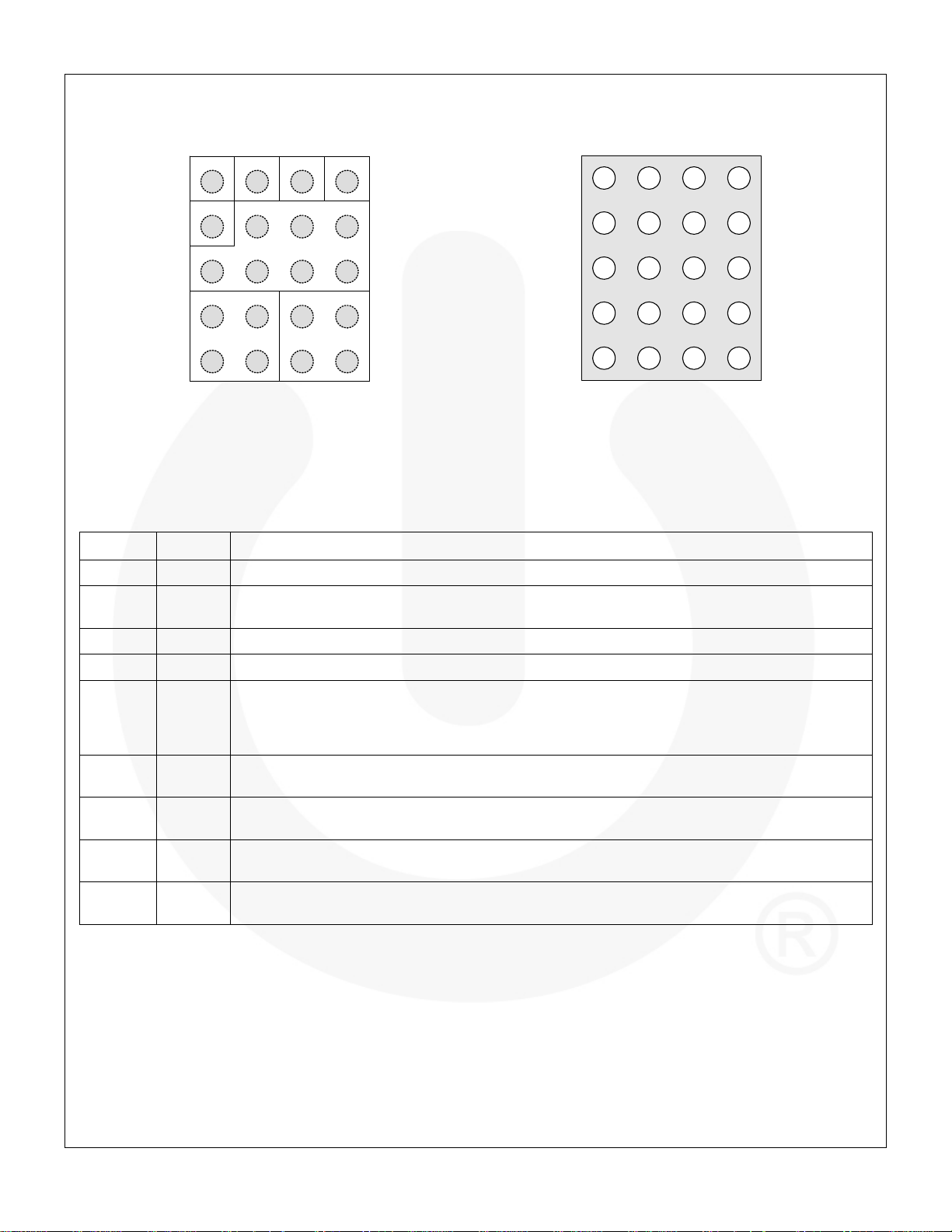
PGOOD
MODE
EN FB VOUT
A1 A2
B1
C1
VIN SW
D1 D3D2
E1 E3E2 E4
B2
C2
A3
GND
B3
C3
A4
B4
C4
D4
Figure 2. Top View Figure 3. Top View Bottom View
Pin Definitions
Bump # Name Description
A1 PGOOD
A2 EN
A3 FB
A4 VOUT
B1 MODE
B2, B3,
C1 – C4
GND
B4 AGND
D1, D2,
E1, E2
D3, D4,
E3, E4
VIN
SW
Power Good. This open-drain pin pulls LOW if the output falls out of regulation or is in soft-start.
Enable. The device is in Shutdown Mode when this pin is LOW. Do not leave this pin floating. When
tying HIGH, use at least a 1kΩ series resistor if V
is expected to exceed 4.5V.
IN
FB. Connect to resistor divider. The IC regulates this pin to 0.8V.
VOUT. Sense pin for V
. Connect directly to C
OUT
OUT
.
MODE / SYNC. A logic 0 allows the IC to automatically switch to PFM during light loads. When held
HIGH, the IC to stays in PWM Mode. The regulator also synchronizes its switching frequency to four
times (4X) the frequency provided on this pin (f
use at least a 1kΩ series resistor if V
is expected to exceed 4.5V.
IN
). Do not leave this pin floating. When tying HIGH,
MODE
Ground. Low-side MOSFET is referenced to this pin. C
path to these pins.
Analog Ground. All signals are referenced to this pin. Avoid routing high dV/dt AC currents through
this pin.
Power Input Voltage. Connect to input power source. Connect to C
Switching Node. Connect to inductor.
A4
B4
C4
D4
and C
IN
B2
C2
A1
B1
C1
D1D3 D2
E1E3 E2E4
A3 A2
B3
C3
should be returned with a minimal
OUT
with minimal path.
IN
© 2011 Fairchild Semiconductor Corporation www.fairchildsemi.com
FAN53540 • Rev. 1.0.2 3
FAN53540 — 2.4 MHz, 5A TinyBuck™ Synchronous Buck Regulator
Absolute Maximum Ratings
Stresses exceeding the absolute maximum ratings may damage the device. The device may not function or be operable above
the recommended operating conditions and stressing the parts to these levels is not recommended. In addition, extended
exposure to stresses above the recommended operating conditions may affect device reliability. The absolute maximum
ratings are stress ratings only.
Symbol Parameter Min. Max. Unit
SW, VIN Pins -0.3 7.0
VIN
ESD
Other Pins
Electrostatic Discharge
Protection Level
Tied without Series Impedance -0.3 4.5
Tied through Series Resistance ≥100
-0.3 V
Human Body Model per JESD22-A114 2250
Charged Device Model per JESD22-C101 1500
TJ Junction Temperature –40 +150 °C
T
Storage Temperature –65 +150 °C
STG
TL Lead Soldering Temperature, 10 Seconds +260 °C
Note:
3. V
4. Lesser of 7V or V
slew rate is limited to 1V/µs.
IN
+0.3V.
IN
(3)
V
IN
V
Recommended Operating Conditions
The Recommended Operating Conditions table defines the conditions for actual device operation. Recommended operating
conditions are specified to ensure optimal performance to the datasheet specifications. Fairchild does not recommend
exceeding them or designing to Absolute Maximum Ratings.
Symbol Parameter Min. Typ. Max. Unit
VIN Supply Voltage Range 2.7 5.5 V
V
Output Voltage Range 0.8 90% Duty Cycle V
OUT
I
Output Current 0 5 A
OUT
L Inductor 0.47 1.20 µH
CIN Input Capacitor 10 µF
C
Output Capacitor 20
OUT
TA Operating Ambient Temperature -40 +85 °C
TJ Operating Junction Temperature -40 +125 °C
μF
Thermal Properties
Symbol Parameter Typical Unit
(5)
JA
Junction-to-Ambient Thermal Resistance 38
Note:
5. See Thermal Considerations in the Applications section.
°C/W
© 2011 Fairchild Semiconductor Corporation www.fairchildsemi.com
FAN53540 • Rev. 1.0.2 4
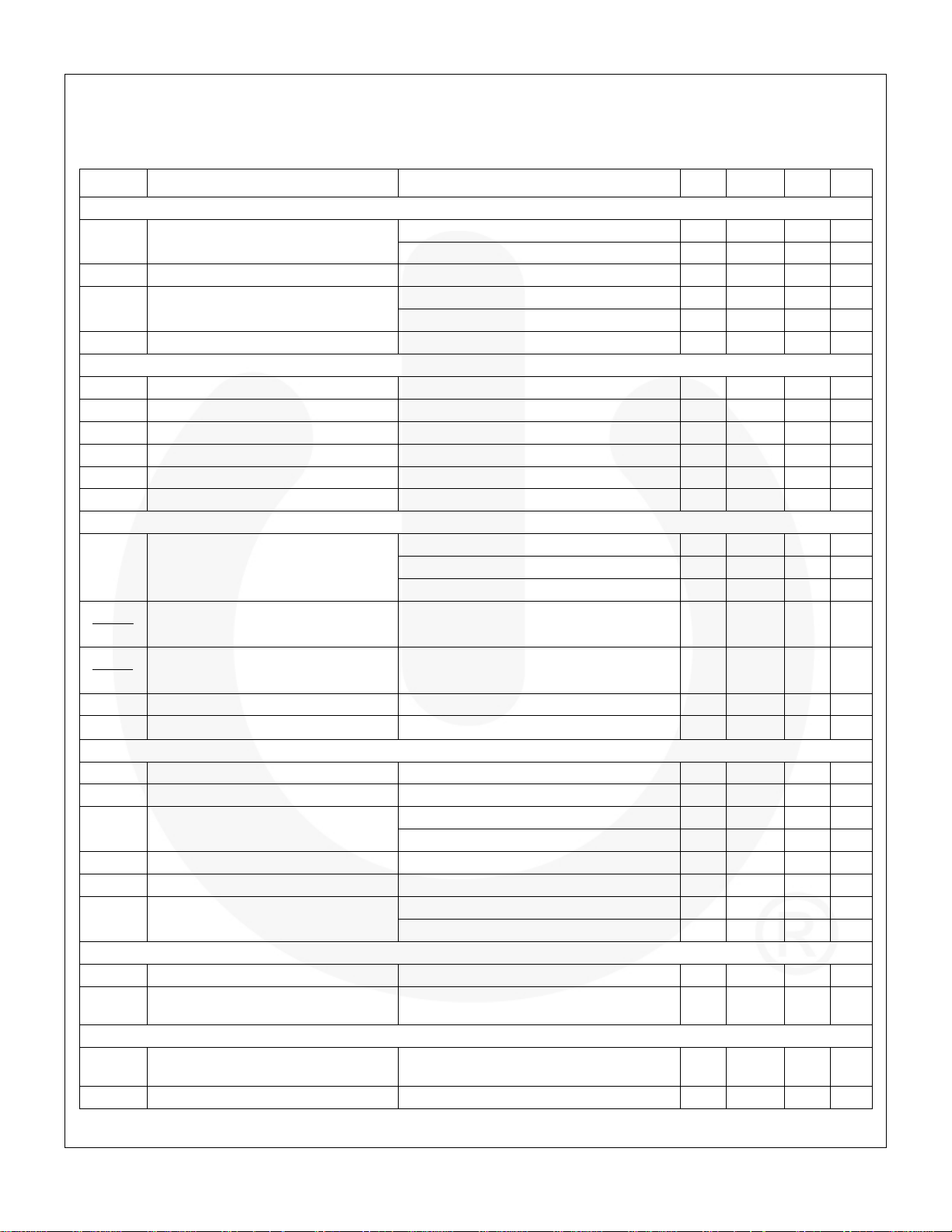
Electrical Characteristics
Minimum and maximum values are at V
=25°C, VIN=5V, and V
T
A
OUT
=1.2V.
Symbol Parameter Condition Min. Typ. Max. Unit
Power Supplies
IQ Quiescent Current
I
Shutdown Supply Current EN=GND 0.1 10 µA
SD
V
Under-Voltage Lockout Threshold
UVLO
V
Logic Pins
V
Power Switch and Protection
R
R
Frequency Control
Soft-Start and Output Discharge
Under-Voltage Lockout Hysteresis 365 mV
UVHYST
VIH High-Level Input Voltage 1.05 V
VIL Low-Level Input Voltage 0.4 V
V
Logic Input Hysteresis Voltage 140 mV
LHYST
IIN Input Bias Current Input Tied to GND or 1ΩK Resistor to VIN 0.01 1.00 µA
I
PGOOD Pull-Down Current V
OUTL
I
PGOOD HIGH Leakage Current V
OUTH
Regulation
OUT
V
IV
I
V
DS(ON)P
DS(ON)N
I
LIMPK
T
T
V
SDWN
Output Reference DC Accuracy,
REF
Measured at FB Pin
OUT
Load Regulation MODE=V
LOAD
OUT
Line Regulation 2.7V ≤ VIN ≤ 5.5V, I
VV
IN
FB Pin Leakage Current FB=0.8V 1 nA
REF
Transient Response I
OUT
P-Channel MOSFET On Resistance 33 mΩ
N-Channel MOSFET On Resistance 28 mΩ
P-MOS Peak Current Limit
Thermal Shutdown 155 °C
LIMIT
Thermal Shutdown Hysteresis 20 °C
HYST
Input OVP Shutdown
fSW Oscillator Frequency 2.1 2.4 3.0 MHz
f
MODE Pin Synchronization Range
MODE
Regulator Enable to Regulated V
tSS
(Rising PGOOD)
R
Output Discharge Resistance EN=0V 175 Ω
DIS
=2.7V to 5.5V, and T
IN
I
=0, MODE=0 (AUTO PFM/PWM) 50 µA
LOAD
I
=0, MODE=1 (Forced PWM) 30 mA
LOAD
V
Rising 2.67 2.80 V
IN
VIN Falling 2.1 2.3 V
PGOOD
PGOOD=VIN
=25°C, Forced PWM 0.792 0.800 0.808 V
T
A
TA=-40°C to 85°C, Forced PWM 0.787 0.800 0.813 V
AUTO PFM/PWM 0.784 0.800 0.824 V
Step 0.1A to 1.5A, tR=100ns -30 mV
LOAD
Open Loop 5.8 7.5 8.8 A
Closed Loop 8 A
Rising Threshold 6.1 V
Falling Threshold 5.5 5.8 V
External Square-Wave, 30% to 70% Duty
Cycle
OUT
1.2 ms
=-40°C to +85°C, unless otherwise noted. Typical values are at
A
=0.4V 1 mA
0.01 1.00 µA
(Forced PWM) –0.02 %/A
IN
=1.5A -0.16 %/V
OUT(DC)
525 600 700 kHz
FAN53540 — 2.4 MHz, 5A TinyBuck™ Synchronous Buck Regulator
© 2011 Fairchild Semiconductor Corporation www.fairchildsemi.com
FAN53540 • Rev. 1.0.2 5
 Loading...