March 2011
FAN5354
3MHz, 3A Synchronous Buck Regulator
FAN5354 — 3MHz, 3A Synchronous Buck Regulator
Features
3MHz Fixed-Frequency Operation
Best-in-Class Load Transient
3A Output Current Capability
2.7V to 5.5V Input Voltage Range
Adjustable Output Voltage: 0.8 to VIN•0.9
PFM Mode for High Efficiency in Light Load (Forced PWM
Available on MODE Pin)
Minimum PFM Frequency Avoids Audible Noise
270µA Typical Quiescent Current in PFM Mode
External Frequency Synchronization
Low Ripple Light-Load PFM Mode with Forced
PWM Control
Power Good Output
Internal Soft-Start
Input Under-Voltage Lockout (UVLO)
Thermal Shutdown and Overload Protection
12-Lead 3x3.5mm MLP
Applications
Description
The FAN5354 is a step-down switching voltage regulator that
delivers an adjustable output from an input voltage supply of
2.7V to 5.5V. Using a proprietary architecture with
synchronous rectification, the FAN5354 is capable of
delivering 3A at over 85% efficiency, while maintaining a
very high efficiency of over 80% at load currents as low as
2mA. The regulator operates at a nominal fixed frequency of
3MHz, which reduces the value of the external components
to 470nH for the output inductor and 10µF for the output
capacitor. Additional output capacitance can be added to
improve regulation during load transients without affecting
stability and inductance up to 1.2µH may be used with
additional output capacitance.
At moderate and light loads, pulse frequency modulation
(PFM) is used to operate the device in power-save mode
with a typical quiescent current of 270µA. Even with such a
low quiescent current, the part exhibits excellent transient
response during large load swings. At higher loads, the
system automatically switches to fixed-frequency control,
operating at 3MHz. In shutdown mode, the supply current
drops below 1µA, reducing power consumption. PFM mode
can be disabled if constant frequency is desired. To avoid
audible noise, the regulator limits its minimum PFM
frequency. The FAN5354 is available in 12-lead 3x3.5mm
MLP package.
Set-Top Box
Hard Disk Drive
Communications Cards
DSP Power
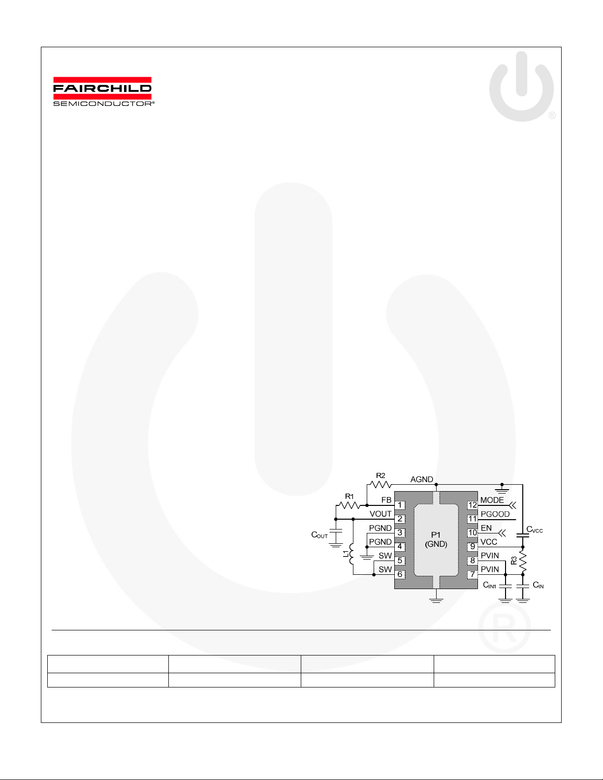
Figure 1. Typical Application
Ordering Information
Part Number Temperature Range Package Packing Method
FAN5354MPX -40 to 85°C MLP-12, 3x3.5mm Tape and Reel
© 2009 Fairchild Semiconductor Corporation www.fairchildsemi.com
FAN5354 • Rev. 1.0.5

Table 1. Recommended External Components for 3A Maximum Load Current
Component Description Vendor Parameter Typ. Units
IHLP1616ABER47M01 (Vishay)
SD12-R47-R (Coiltronics)
L1 470nH Nominal
VLC5020T-R47N (TDK)
(TDK)
LQH55PNR47NT0 (Murata)
C
C
C
C
R3
OUT
IN
IN1
VCC
10nF, 25V, X7R, 0402
(1)
4.7µF, 6.3V, X5R, 0603
2 Pieces
10µF, 6.3V, X5R, 0805
10µF, 6.3V, X5R, 0805
Resistor: 1Ω 0402
GRM21BR60J106M (Murata)
C2012X5R0J106M (TDK)
GRM155R71E103K (Murata)
C1005X7R1E103K (TDK)
GRM188R60J475K (Murata)
C1608X5R0J475K (TDK)
Any R 1
Note:
1. R3 is optional and improves IC power supply noise rejection. See Layout recommendations for more information.
L 0.47
DCR 20
C 10.0
C 10 nF
C 4.7
µH
mΩ
µF
µF
Ω
Pin Configuration
FAN5354 — 3MHz, 3A Synchronous Buck Regulator
FB
VOU T
PGN D
PGN D
SW
SW
1
2
3
4
5
P1
(GND)
12
11
10
9
8
7
MODE
PGO OD
EN
VCC
PVIN
PVIN6
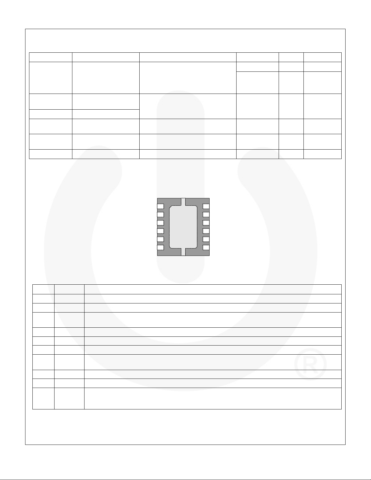
Figure 2. 12-Pin, 3x3.5mm MLP (Top View)
Pin Definitions
Pin # Name Description
1 FB
2 VOUT
3, 4 PGND
5, 6 SW
P1 GND
7, 8 PVIN
9 VCC
10 EN
11 PGOOD
12 MODE
Note:
2. P1 is the bottom heat-sink pad. Ground plane should flow through pins 3, 4, and P1 and can be extended through pin 11 if
PGOOD’s function is not required, and through pin 12 if MODE is to be grounded, to improve IC cooling.
FB. Connect to resistor divider. The IC regulates this pin to 0.8V.
VOUT. Sense pin for VOUT. Connect to COUT.
Power Ground. Low-side MOSFET is referenced to this pin. CIN and COUT should be returned with a
minimal path to these pins.
Switching Node. Connect to inductor.
Ground. All signals are referenced to this pin.
Power Input Voltage. Connect to input power source. Connect to CIN with minimal path.
IC Bias Supply. Connect to input power source. Use a separate bypass capacitor CVCC from this pin
to the P1 GND terminal between pins 1 and 12.
Enable. The device is in shutdown mode when this pin is LOW. Do not leave this pin floating.
Power Good. This open-drain pin pulls LOW if the output falls out of regulation or is in soft-start.
MODE / Sync. A logic 0 allows the IC to automatically switch to PFM during light loads. When held
HIGH, the IC to stays in PWM mode. The regulator also synchronizes its switching frequency to the
frequency provided on this pin. Do not leave this pin floating.
© 2009 Fairchild Semiconductor Corporation www.fairchildsemi.com
FAN5354 • Rev. 1.0.5 2

Absolute Maximum Ratings
Stresses exceeding the absolute maximum ratings may damage the device. The device may not function or be operable above
the recommended operating conditions and stressing the parts to these levels is not recommended. In addition, extended
exposure to stresses above the recommended operating conditions may affect device reliability. The absolute maximum
ratings are stress ratings only.
Symbol Parameter Min. Max. Units
VIN
SW, PVIN, VCC Pins
Other Pins -0.3 VCC + 0.3
V
INOV_SLEW
R
PGOOD
ESD
Maximum Slew Rate of VIN Above 6.5V when PWM is Switching 15 V/ms
Pull-Up Resistance from PGOOD to VCC 1
Electrostatic Discharge
Protection Level
TJ Junction Temperature –40 +150 °C
T
Storage Temperature –65 +150 °C
STG
TL Lead Soldering Temperature, 10 Seconds +260 °C
Note:
3. Lesser of 7V or VCC+0.3V.
IC Not Switching -0.3 7.0
IC Switching -0.3 6.5
Human Body Model per JESD22-A114 2
Charged Device Model per JESD22-C101 2
V
(3)
V
KΩ
KV
FAN5354 — 3MHz, 3A Synchronous Buck Regulator
Recommended Operating Conditions
The Recommended Operating Conditions table defines the conditions for actual device operation. Recommended operating
conditions are specified to ensure optimal performance to the datasheet specifications. Fairchild does not recommend
exceeding them or designing to Absolute Maximum Ratings.
Symbol Parameter Min. Typ. Max. Units
V
Supply Voltage Range 2.7 5.5 V
CC, VIN
V
Output Voltage Range 0.8 90% Duty Cycle V
OUT
I
Output Current 0 3 A
OUT
L Inductor 0.47 µH
CIN Input Capacitor 10 µF
C
Output Capacitor 20 µF
OUT
TA Operating Ambient Temperature -40 +85 °C
TJ Operating Junction Temperature -40 +125 °C
Thermal Properties
Symbol Parameter Min. Typ. Max. Units
θJA
Junction-to-Ambient Thermal Resistance
Note:
4. Junction-to-ambient thermal resistance is a function of application and board layout. This data is measured with four-layer
1s2p boards in accordance to JESD51- JEDEC standard. Special attention must be paid not to exceed junction
temperature T
at a given ambient temperate TA.
J(max)
(4)
46 °C/W
© 2009 Fairchild Semiconductor Corporation www.fairchildsemi.com
FAN5354 • Rev. 1.0.5 3

Electrical Characteristics
Minimum and maximum values are at VIN=2.7V to 5.5V, TA=-40°C to +85°C, unless otherwise noted. Typical values are at
TA=25°C, VIN=5V.
Symbol Parameter Conditions Min. Typ. Max. Units
Power Supplies
I
=0, MODE=0 270
IQ Quiescent Current
I
Shutdown Supply Current EN=GND 0.1 3.0
SD
V
Under-Voltage Lockout Threshold
UVLO
V
Under-Voltage Lockout Hysteresis 530 mV
UVHYST
LOAD
I
=0, MODE=1 (Forced PWM) 14 mA
LOAD
VIN Rising 2.83 2.95 V
VIN Falling 2.10 2.30 2.40 V
Logic Pins
VIH HIGH-Level Input Voltage 1.05 V
VIL LOW-Level Input Voltage 0.4 V
V
Logic Input Hysteresis Voltage 100 mV
LHYST
IIN Input Bias Current Input Tied to GND or VIN 0.01 1.00
I
PGOOD Pull-Down Current V
OUTL
I
PGOOD HIGH Leakage Current V
OUTH
V
Regulation
OUT
V
V
∆
IV∆
∆
Output Reference DC Accuracy
REF
Measured at FB Pin
REG
OUT
LOAD
OUT
VV∆
IN
V
DC Accuracy
OUT
Load Regulation I
Line Regulation 2.7V ≤ VIN ≤ 5.5V, I
Transient Response I
=0.4V 1 mA
PGOOD
PGOOD=VIN
0.01 1.00
TA=25°C 0.792 0.800 0.808 V
0.788 0.800 0.812 V
At V
Pin W.R.T. Calculated Value,
OUT
I
=500mA
LOAD
=1 to 3A –0.03 %/A
OUT(DC)
=1.5A 0.01 %/V
OUT(DC)
Step 0.1A to 1.5A, tr=tf=100ns, V
LOAD
=1.2V +40 mV
OUT
1.6 +1.6 %
Power Switch and Protection
R
DS(ON)P
R
DS(ON)N
I
LIMPK
T
T
V
SDWN
P-Channel MOSFET On Resistance 60 mΩ
N-Channel MOSFET On Resistance 40 mΩ
P-MOS Peak Current Limit 3.75 4.55 5.50 A
Thermal Shutdown 150 °C
LIMIT
Thermal Shutdown Hysteresis 20 °C
HYST
Input OVP Shutdown
Rising Threshold 6.2 V
Falling Threshold 5.50 5.85 V
Frequency Control
fSW Oscillator Frequency 2.7 3.0 3.3 MHz
f
MODE Pin Synchronization Range External Square-Wave, 30% to 70% Duty Cycle 2.7 3.0 3.3 MHz
SYNC
f
Minimum PFM Frequency TA = 25°C, V
PFM(MIN)
= 5.0V 17 26 36 kHz
IN
Soft-Start
tSS Regulator Enable to Regulated V
V
Soft-Start V
SLEW
Slew Rate 10 V/ms
REF
OUT
R
> 5Ω, to V
LOAD
R
> 5Ω, to V
LOAD
OUT
OUT
=1.2V
=1.8V
210 250
340 420
µA
µA
µA
µA
µs
µs
FAN5354 — 3MHz, 3A Synchronous Buck Regulator
© 2009 Fairchild Semiconductor Corporation www.fairchildsemi.com
FAN5354 • Rev. 1.0.5 4

FAN5354 — 3MHz, 3A Synchronous Buck Regulator
OUT
Figure
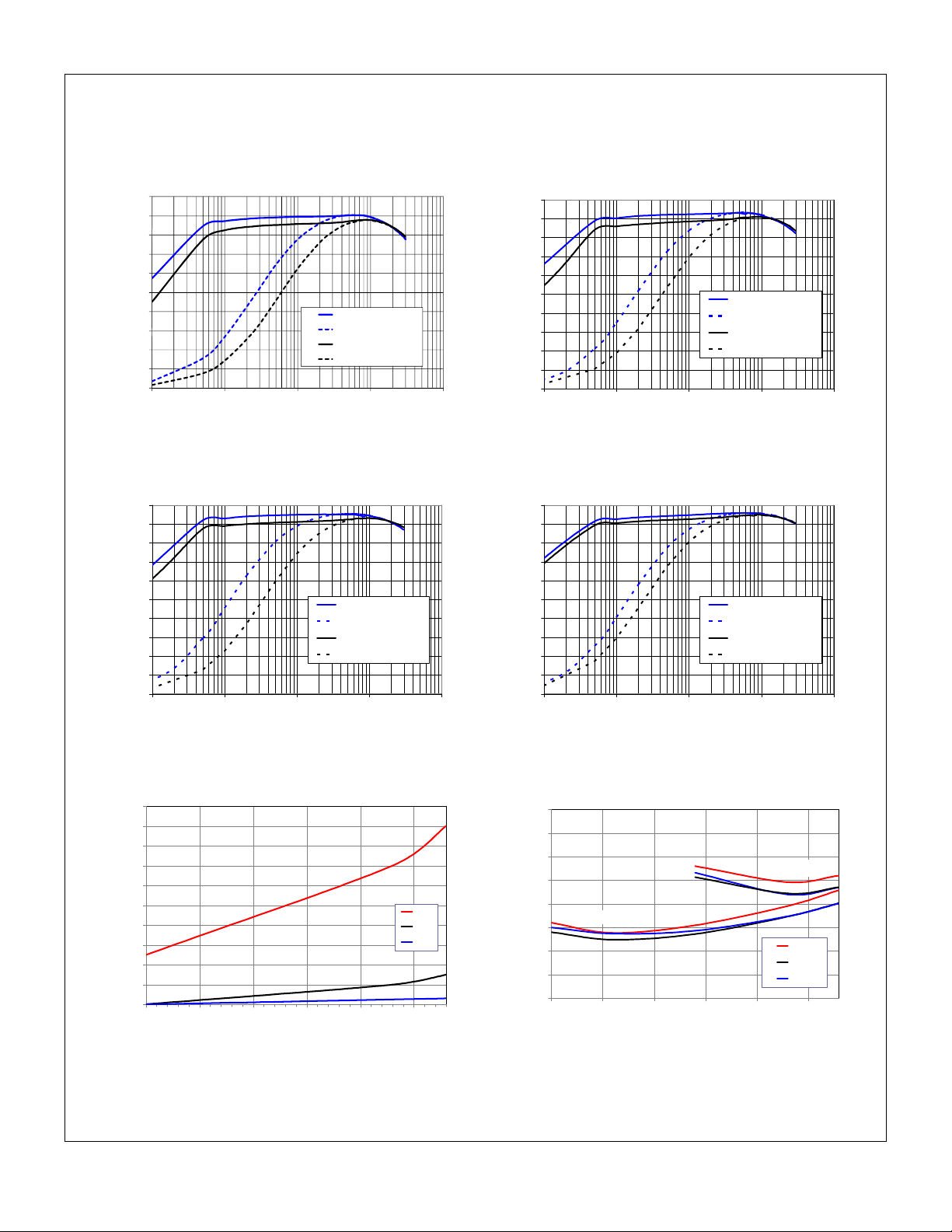
3. Efficiency vs. I
LOAD
at V
OUT
=1.2V
Figure
4.
Efficiency vs. I
LOAD
at
V
OUT
=
1.8V
Figure
5.
Efficiency vs. I
LOAD
at
V
OUT
=
2.5V Figure
6.
Efficiency vs. I
LOAD
at
V
OUT
=
3.3V
Typical Characteristics
Unless otherwise specified, VIN=5V, V
100%
90%
80%
70%
60%
50%
40%
Efficiency
30%
20%
10%
0%
1 10 100 1000 10000
I
Output Current (mA)
LOAD
100%
90%
80%
70%
60%
50%
40%
Efficiency
30%
20%
10%
0%
1 10 100 1000 10000
I
Output Current (mA)
LOAD
=1.2V, circuit of Figure 1, and components per Table 1.
100%
90%
80%
70%
60%
50%
40%
VIN = 3.3V, Mode=0
VIN = 3.3V, Mode=1
VIN = 5V, Mode=0
VIN = 5V, Mode=1
VIN = 3.3V, Mode = 0
VIN = 3.3V, Mode = 1
VIN = 5V, Mode = 0
VIN = 5V, Mode = 1
Efficiency
30%
20%
10%
0%
1 10 100 1000 10000
I
Output Current (mA)
LOAD
100%
90%
80%
70%
60%
50%
40%
Efficiency
30%
20%
10%
0%
1 10 100 1000 10000
I
Output Current (mA)
LOAD
VIN = 3.3V, Mode = 0
VIN = 3.3V, Mode = 1
VIN = 5V, Mode = 0
VIN = 5V, Mode = 1
VIN = 4.2V, Mode = 0
VIN = 4.2V, Mode = 1
VIN = 5V, Mode = 0
VIN = 5V, Mode = 1
© 2009 Fairchild Semiconductor Corporation www.fairchildsemi.com
FAN5354 • Rev. 1.0.5 5
1
0.9
0.8
0.7
A)
µ
µ
µ
µ
0.6
0.5
0.4
0.3
Supply Current (
0.2
0.1
0
2.7 3.2 3.7 4.2 4.7 5.2
Input Voltage(V)
85°C
25°C
-40°C
400
375
350
325
300
275
250
PFM, No load supply Current(µA)
225
200
VOUT = 1.2
2.7 3.2 3.7 4.2 4.7 5.2
Input Voltage(V)
VOUT = 3.3
85°C
25°C
–40°C
Figure 7. Shutdown Supply Current vs VIN, EN=0 Figure 8. Quiescent Current in PFM vs. VIN, No Load
 Loading...