Fairchild FAN5353 service manual

FAN5353 — 3MHz, 3A Synchronous Buck Regulator
September 2010
FAN5353
3MHz, 3A Synchronous Buck Regulator
Features
3MHz Fixed-Frequency Operation
Best-in-Class Load Transient
3A Output Current Capability
2.7V to 5.5V Input Voltage Range
Adjustable Output Voltage: 0.8V to V
IN
•0.9
Power Good Output
Internal Soft-Start
Input Under-Voltage Lockout (UVLO)
Thermal Shutdown and Overload Protection
12-lead 3x3.5mm MLP
Applications
Set-Top Box
Hard Disk Drive
Communications Cards
DSP Power
Description
The FAN5353 is a step-down switching voltage regulator that
delivers an adjustable output from an input voltage supply of
2.7V to 5.5V. Using a proprietary architecture with
synchronous rectification, the FAN5353 is capable of
delivering 3A at over 85% efficiency. The regulator operates
at a nominal fixed frequency of 3MHz, which reduces the
value of the external components to 470nH for the output
inductor and 10µF for the output capacitor. Additional output
capacitance can be added without affecting stability if tighter
regulation during transients is required. The regulator
includes an open-drain power good (PGOOD) signal that
pulls low when the output is not in regulation.
In shutdown mode, the supply current drops below 1µA,
reducing power consumption.
FAN5353 is available in a 12-lead 3x3.5mm MLP package.
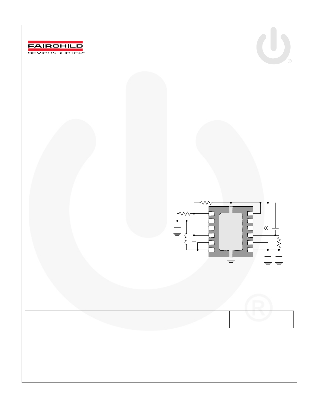
R1
C
OUT
L1
FB
VOUT
PGND
PGND
SW
SW
R2
1
2
3
4
5
6
AGND
(GND)
P1
12
11
10
9
8
7
PGOOD
EN
VCC
PVIN
PVIN
C
IN1
R3
C
VCC
C
IN
Figure 1. Typical Application
Ordering Information
Part Number Temp. Range Package Packing Method
FAN5353MPX -40 to 85°C MLP-12, 3x3.5mm Tape and Reel
© 2009 Fairchild Semiconductor Corporation www.fairchildsemi.com
FAN5353 • Rev. 1.0.2

FAN5353 — 3MHz, 3A Synchronous Buck Regulator
Table 1. Recommended External Components for 3A Maximum Load Current
Component Description Vendor Parameter Typ. Units
Vishay IHLP1616ABER47M01
L1 470nH nominal
Coiltronics SD12-R47-R
TDK VLC5020T-R47N
MURATA LQH55PNR47NT0
C
C
C
C
R3
OUT
IN
IN1
VCC
(1)
4.7μF, 6.3V, X5R, 0603
2 pieces
10μF, 6.3V, X5R, 0805
10μF, 6.3V, X5R, 0805
10nF, 25V, X7R, 0402
Resistor: 1Ω 0402
GRM21BR60J106M (Murata)
C2012X5R0J106M (TDK)
GRM155R71E103K (Murata)
C1005X7R1E103K (TDK)
GRM188R60J475K (Murata)
C1608X5R0J475K (TDK)
any R 1
Note:
1. R3 is optional and improves IC power supply noise rejection. See Layout recommendations for more information.
L 0.47
DCR 20
C 10.0
μH
mΩ
μF
C 10 nF
C 4.7
μF
Ω
Pin Configuration
FB
VOUT
PGND
PGND
SW
SW
1
2
3
4
5
6
P1
(GND)
12
11
10
9
8
7
NC
PGOOD
EN
VCC
PVIN
PVIN
Figure 2. 12-Pin, 3x3.5mm MLP (Top View)
Pin Definitions
Pin # Name Description
1 FB
2 VOUT
3, 4 PGND
5, 6 SW
P1 GND
7, 8 PVIN
9 VCC
10 EN
11 PGOOD
12 NC This pin has no function and should be tied to GND.
Note:
2. P1 is the bottom heat-sink pad. Ground plane should flow through pins 3, 4, 12, and P1 and can be extended through pin
11 if PGOOD’s function is not required to improve IC cooling.
FB. Connect to resistor divider. The IC regulates this pin to 0.8V.
VOUT. Sense pin for VOUT. Connect to COUT.
Power Ground. Low-side MOSFET is referenced to this pin. CIN and COUT should be returned with a
minimal path to these pins.
Switching Node. Connect to inductor.
Ground. All signals are referenced to this pin.
Power Input Voltage. Connect to input power source. Connect to CIN with minimal path.
IC Bias Supply. Connect to input power source. Use a separate bypass capacitor CVCC from this pin
to the P1 GND terminal between pins 1 and 12.
Enable. The device is in shutdown mode when this pin is LOW. Do not leave this pin floating.
Power Good. This open-drain pin pulls LOW if the output falls out of regulation or is in soft-start.
© 2009 Fairchild Semiconductor Corporation www.fairchildsemi.com
FAN5353 • Rev. 1.0.2 2

FAN5353 — 3MHz, 3A Synchronous Buck Regulator
Absolute Maximum Ratings
Stresses exceeding the absolute maximum ratings may damage the device. The device may not function or be operable above
the recommended operating conditions and stressing the parts to these levels is not recommended. In addition, extended
exposure to stresses above the recommended operating conditions may affect device reliability. The absolute maximum
ratings are stress ratings only.
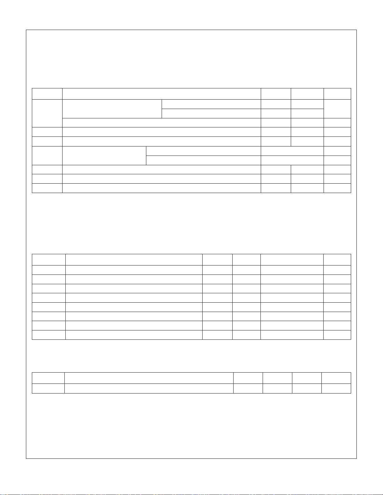
Symbol Parameter Min. Max. Units
VIN
SW, PVIN, VCC Pins
Other Pins -0.3 VCC + 0.3
V
INOV_SLEW
R
Maximum Slew Rate of VIN Above 6.5V when PWM is Switching 15 V/ms
Pull-Up Resistance from PGOOD to VCC 1
PGOOD
ESD
Electrostatic Discharge
Protection Level
TJ Junction Temperature –40 +150 °C
T
Storage Temperature –65 +150 °C
STG
TL Lead Soldering Temperature, 10 Seconds +260 °C
Note:
3. Lesser of 7V or V
+0.3V.
CC
IC Not Switching -0.3 7.0
IC Switching -0.3 6.5
V
(3)
V
KΩ
Human Body Model per JESD22-A114 2 KV
Charged Device Model per JESD22-C101 2 KV
Recommended Operating Conditions
The Recommended Operating Conditions table defines the conditions for actual device operation. Recommended operating
conditions are specified to ensure optimal performance to the datasheet specifications. Fairchild does not recommend
exceeding them or designing to Absolute Maximum Ratings.
Symbol Parameter Min. Typ. Max. Units
V
Supply Voltage Range 2.7 5.5 V
CC, VIN
V
Output Voltage Range 0.8 90% Duty Cycle V
OUT
I
Output Current 0 3 A
OUT
L Inductor 0.47 µH
CIN Input Capacitor 10 µF
C
Output Capacitor 20 µF
OUT
TA Operating Ambient Temperature -40 +85 °C
TJ Operating Junction Temperature -40 +125 °C
Thermal Properties
Symbol Parameter Min. Typ. Max. Units
θJA
Junction-to-Ambient Thermal Resistance
Note:
4. Junction-to-ambient thermal resistance is a function of application and board layout. This data is measured with four-layer
1s2p boards in accordance to JESD51- JEDEC standard. Special attention must be paid not to exceed junction
temperature T
at a given ambient temperate TA.
J(max)
(4)
46 °C/W
© 2009 Fairchild Semiconductor Corporation www.fairchildsemi.com
FAN5353 • Rev. 1.0.2 3

FAN5353 — 3MHz, 3A Synchronous Buck Regulator
Electrical Characteristics
Minimum and maximum values are at V
= 25°C, VIN =5V.
T
A
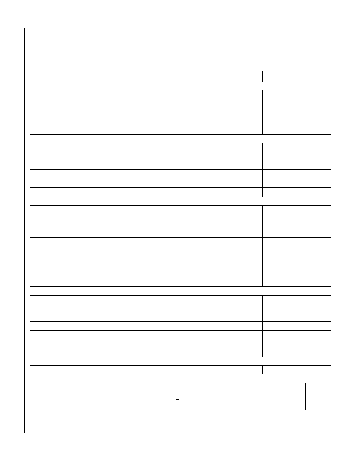
Symbol Parameter Conditions Min. Typ. Max. Units
Power Supplies
IQ Quiescent Current I
I
Shutdown Supply Current EN = GND 0.1 3.0
SD
V
Under-Voltage Lockout Threshold
UVLO
V
Logic Pins
VOUT Regulation
Power Switch and Protection
R
R
Frequency Control
Soft-Start
Under-Voltage Lockout Hysteresis 530 mV
UVHYST
VIH HIGH-Level Input Voltage 1.05 V
VIL LOW-Level Input Voltage 0.4 V
V
Logic Input Hysteresis Voltage 100 mV
LHYST
IIN Input Bias Current Input tied to GND or VIN 0.01 1.00
I
PGOOD Pull-Down Current V
OUTL
I
PGOOD HIGH Leakage Current V
OUTH
Output Reference DC Accuracy
Measured at FB Pin
V
OUT
OUT
IN
DC Accuracy
OUT
Load Regulation I
Line Regulation
Δ
Δ
V
V
IVΔ
LOAD
REF
REG
VVΔ
Transient Response
P-channel MOSFET On Resistance 60 mΩ
DS(ON)P
N-channel MOSFET On Resistance 40 mΩ
DS(ON)N
I
P-MOS Peak Current Limit 3.75 4.55 5.50 A
LIMPK
T
Thermal Shutdown 150 °C
LIMIT
T
Thermal Shutdown Hysteresis 20 °C
HYST
V
Input OVP Shutdown
SDWN
fSW Oscillator Frequency 2.7 3.0 3.3 MHz
tSS Regulator Enable to Regulated V
V
Soft-Start V
SLEW
Slew Rate 10 V/ms
OUT
= 2.7V to 5.5V, T
IN
OUT
= -40°C to +85°C, unless otherwise noted. Typical values are at
A
LOAD
= 0, V
=1.2V 14 mA
OUT
μA
V
Rising 2.83 2.95 V
IN
VIN Falling 2.10 2.30 2.40 V
μA
= 0.4V 1 mA
PGOOD
= VIN 0.01 1
PGOOD
= 25°C 0.792 0.800 0.808 V
T
A
μA
0.788 0.800 0.812 V
At VOUT pin W.R.T. Calculated
Value, I
OUT(DC)
2.7V ≤ V
= 500mA
LOAD
= 0 to 3A –0.03 %/A
≤ 5.5V, I
IN
OUT(DC)
=
1.5A
I
step 0.1A to 1.5A, tr = tf =
LOAD
100ns, V
OUT
=1.2V
1.6% +1.6 %
0.01 %/V
+20 mV
Rising Threshold 6.2 V
Falling Threshold 5.50 5.85 V
R
R
LOAD
LOAD
> 5Ω, to V
> 5Ω, to V
OUT
OUT
= 1.2V
= 1.8V
210 250
340 420
μs
μs
© 2009 Fairchild Semiconductor Corporation www.fairchildsemi.com
FAN5353 • Rev. 1.0.2 4
 Loading...