Fairchild FAN5336 service manual

April 2009
FAN5336
1.5MHz TinyBoost™ Regulator with 33V Integrated
FET Switch
FAN5336 — 1.5MHz TinyBoost™ Regulator with 33V Integrated FET Switch
Features
■ 1.5MHz Switching Frequency
■ Low Noise
■ Adjustable Output Voltage
■ Up to 1.5A Peak Switch Current
■ Low Shutdown Current: <1µA
■ Cycle-by-Cycle Current Limit
■ Over-Voltage Protection at the Feedback Pin
■ Fixed-Frequency PWM Operation
■ Soft-Start Capabilit y
■ Internal Compensation
■ Thermal Shu tdown
■ Excellent Load Regulation: 0.2%
■ Low Ripple
■ 6-Lead 3x3mm MLP
Applications
■ Portable Displays
■ Mobile Phone / Smart Phone LED Backlights
■ Display Bias
■ PDA, DVD, Camcorder Backlights
■ Pager and Cordless Phone Displays
■ Portable Medical Diagnostic Equipment
■ Remote Controls
■ MP3 or PMP or DSC Players
■ Serial Flash LED Drivers
Description
The FAN5336 is a high-efficiency, low-noise, fixed-frequency PWM, current-mode, DC-DC boost regulator. It
is designed for small LCD bias supply and white LED
backlight supply applications. Depending on the application, a FAN5336 regulator can output up to 33V at up to
50mA output current. With output voltage up to 21V, the
output current can be up to 100mA. FAN5336 can be
used for power conversion as low as 9V output voltage.
A current-mode control loop has a fast transient
response that provides excellent load regulation within
0.2% of output voltage. The FAN5336 switches at fixed
1.5MHz frequency, allowing the use of small, low-cost
external components. Constant frequency switching
results in low input noise and small output capacitors.
FAN5336 provides cycle-by-cycle current limiting up to
1.5A peak current.
The FAN5336 may be used to drive a serial flash LED
with up to 100mA current at 21V for a maximum of
400ms on-time and 10% duty cycle.
A low-EMI mode reduces interference and radiated electromagnetic energy cau sed by the ringin g of the inductor .
Additional features include thermal shutdown, over-voltage protection, cycle-by-cycle current limit, low ripple,
and soft-start support.
The device is available i n a 3x3mm 6-le ad MLP, 0.8mm
thickness package.
Application Diagram
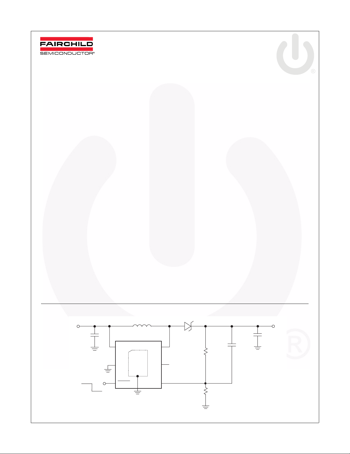
V
IN
C
IN
10µF
ON
OFF
1
2
3
V
IN
GND
SHDN
L1
6.8µH
P1
SW
NC
FB
6
5
4
Figure 1. Typical Application Diagram
© 2004 Fairchild Semiconductor Corporation www.fairchildsemi.com
FAN5336 Rev. 1.0.2
D1
R1
R2
C
F
180pF
C
OUT
4.7µF
V
OUT

Ordering Information
Part Number Package Temperature Range Eco Status Packing Method
FAN5336MPX 6-Lead 3x3mm MLP -40°C to +85°C Green Tape and Reel
FAN5336UMPX 6-Lead 3x3mm UMLP -40°C to +8 5°C Green Tape and Reel
For Fairchild’s definition of “green” Eco Status, please visit: http://www.fairchildsemi.com/company/green/rohs_green.html.
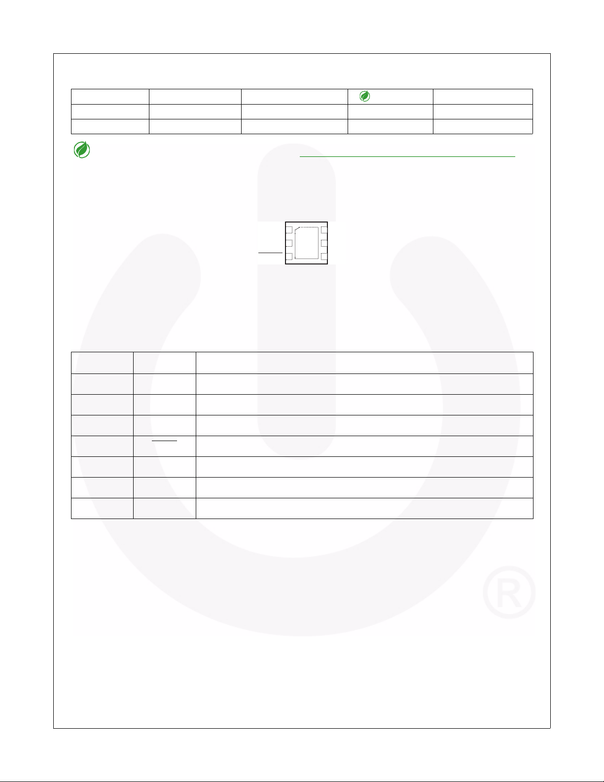
Pin Assignments
1
VIN
2
GND
SHDN
3
Figure 2. 6-Lead, 3x3mm MLP (Top View)
P1
6
SW
5
NC
4
FB
FAN5336 — 1.5MHz TinyBoost™ Regulator with 33V Integrated FET Switch
Pin Descriptions
Pin # Name Description
P1 GND Analog and Power Ground. P1 must be soldered to the PCB ground.
1V
2 GND Ground.
3 SHDN
4FB Feedback Pin. Feedback node that connects to an external voltage divider.
5 NC No Connect.
6 SW Switching Node.
Input Voltage Pin.
IN
Shutdown Control Pin. Logic HIGH enables, logic LOW disables the device.
© 2004 Fairchild Semiconductor Corporation www.fairchildsemi.com
FAN5336 Rev. 1.0.2 2

Absolute Maximum Ratings
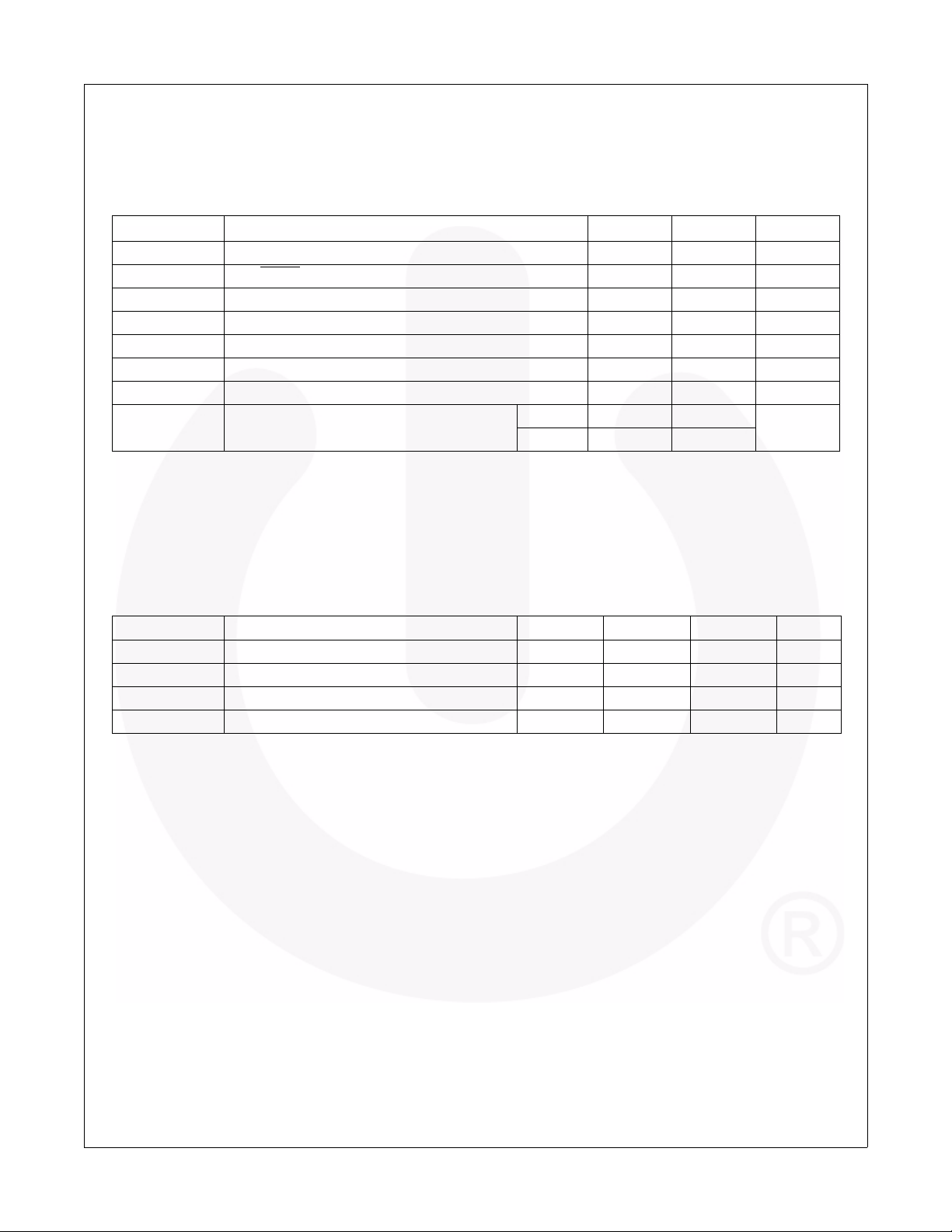
Stresses exceeding the absolute maximum ratings may damage the device. The device may not function or be operable above the recommend ed op erati ng cond iti ons and stres si ng the p arts to these levels is not recommended. In addition, extended exposure to stresses above the recommended operating conditions may affect device reliability. The
absolute maximum ratings are stress ratings only.
Symbols Parameter Min. Max. Unit
V
IN
T
L
T
J
T
STG
Θ
JA
ESD Electrostatic Discharge Protection Level
Note:
1. Using EIA/JESD22A114B (Human Body Model) and EIA/JESD22C101-A (Charge Device Model).
VIN to GND 6.0 V
FB, SHDN
to GND -0.3 VIN + 0.3 V
SW to GND -0.3 35 V
Lead Soldering Temperature (10 seconds) 300 °C
Junction Temperature 150 °C
Storage Temperature -55 150 °C
Thermal Resistance 265 °C/W
HBM 2
(1)
CDM 1
kV
FAN5336 — 1.5MHz TinyBoost™ Regulator with 33V Integrated FET Switch
Recommended Operating Conditions
The Recommended Operating Conditions table defines the conditions for actual device operation. Recommended
operating conditions are specified to ensure optimal performance to the datasheet specifications. Fairchild does not
recommend exceeding them or designing to absolute maximum ratings.
Symbols Parameter Min. T y p. Max. Unit
V
IN
V
OUT
T
A
C
OUT
Note:
2. This load capacitanc e value is required for l oop stability. Toleran ce, temperature vari ation, and voltage de pendency
of the capacitance must be considered. Typically a 4.7µF ceramic capacitor is required to achieve the specified
value at V
Input Voltage 2.7 5.5 V
Output Voltage 9 33 V
Ambient Operating Temperature -40 25 85 °C
Output Capacitance 2.2
= 33V.
OUT
(2)
10 µF
© 2004 Fairchild Semiconductor Corporation www.fairchildsemi.com
FAN5336 Rev. 1.0.2 3
 Loading...