Fairchild FAN5069 service manual

www.fairchildsemi.com
AN-6010
FAN5069 Component Calculation and Simulation Tools
Background / Overview
This app note describes design tools for FAN5069,
which include:
• An Excel workbook to calculate recommended external
component values
• A continuous-time behavioral model of the modulator
that runs in PSPICE A/D v 9.1 or above. The model is
small enough to run under Cadence's Orca d Lit e
Edition (includes Orcad Capture and PSPICE A/D),
which can be ordered on CD at
HTUhttp://www.ema-eda.com/products/Default.aspxUHT
or downloaded from:
HTUhttp://www.orcad.com/download.orcaddemo.aspxUHT.
Note: These links have been verified as of this
publication date, but may change over time.
These design aids (including this document) can be
downloaded from:
HTUhttp://www.fairchildsemi.com/collateral/AN-6010.zipUTH.
To install, copy AN-6010.ZIP to an empty folder (e.g.
“FAN5069Design”), then unzip / extract AN-6010.ZIP into
that folder.
This tool set applies to the following products:
FAN5069
HTUhttp://www.fairchildsemi.com/pf/FA/FAN5069.htmlUHT
Spreadsheet Start-up
The spreadsheet uses functions in Excel’s Analysis ToolPak
add-in to optimize compensation and installs it
automatically if it is not already installed.
Some Excel installations may not have Analysis ToolPak
included. If the following message appears, run Microsoft
Office installation to make the Analysis ToolPak add-in
available.
Consult your Microsoft Excel documentation for
information should this error occur.
Macro Security Note
FAN5069 Design calculation aid.xls uses macros
extensively. For the spreadsheet to operate properly, check
the “Always trust macros from this source” box if a security
warning appears, then click the Enable Macros button.
This is only required the first time you run a Fairchild
spreadsheet tool with macros.
Design Procedure
1. Use the spreadsheet (FAN5069 Design calculation
aid.xls ). The “Instructions” tab provides det ai l ed
instructions for the spreadsheet.
2. After completing the “Component Selection” tab, the
regulator’s small signal response can be viewed in the
“Bode Plot” tab.
3. Verify transient and small signal stability using the
PSPICE Simulation Model provided, using the
components chosen in the “Component Selection” tab.
Note: There will be minor differences between the PSPICE
and Spreadsheet bode plots. The PSPICE model has a more
accurate representation of the IC.
© 2006 Fairchild Semiconductor Corporation www.fairchildsemi.com
Rev. 1.0.5 • 7/7/06

AN-6010 APPLICATION NOTE
PSPICE Simulation Model
The simulation model is a sampled-data, continuous-time
model, which is adapted from Ray Ridley and Dennis
Feucht's modeling work for current mode controllers
The model provides a bode plot where the red trace is phase
margin (in degrees) and the green trace is gain (in dB). The
model also provides transient response using a pulsed
current source (Istep) as the load. The IC’s error-amp
behavioral model is based on Ray Kendall’s
Macromodelling article in EDN.
PDivDP
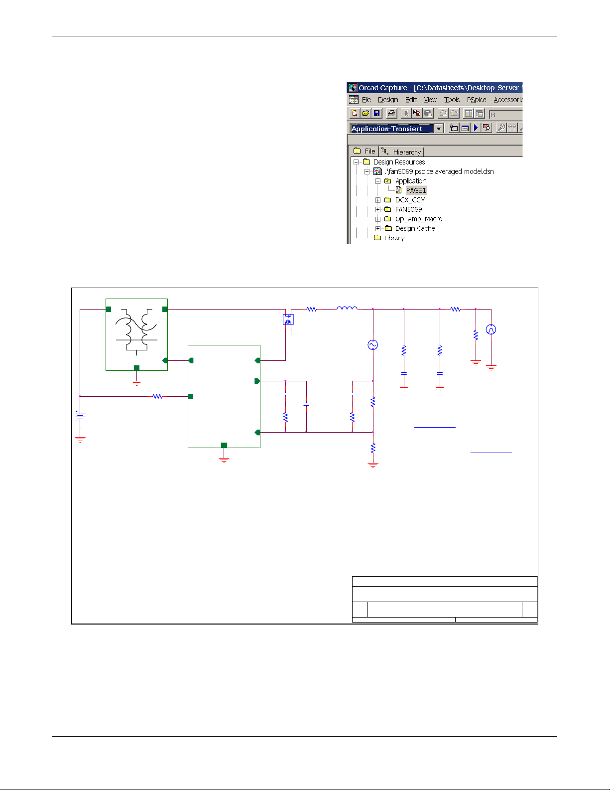
1. To run the model, start Capture (9.1 or higher).
2. Open FAN5069 PSpice Avg Model.opj.
i
PD
DP,PDiiDP,PD
iii
DP.
3. Double-click on Page 1 under: \FAN5 069 pspice avg
model.dsn\Application.
Time_Avg_SW
In
Vin
{Vin}
0
A C
P
DCX_CCM
0
D
Rramp
{Rramp}
SW
F1
F
D
D
RAMP
FAN5069
SW
COMP
U1
PGND
C1
{C1}
R2
{R2}
FB
0
Application Circuit
Notes:
(1) Reset RLoad to desired value when switching
between AC sweep and transient simulation.
(2) For more accurate AC swe e p, descend into U1
an d set Esampling XFORM to 1+s/(wn*Q z)+ (s/wn )* * 2.
(3) For transient analysis, set XFORM to 1.
1 2
{R3}
FB
{C3}
L1
{L}
C3
R3
Rdc
{L_ESR}
0
C2
{C2}
Expressions for Probe
to generate Bode plot:
DB(V(Out)/V(SENSE))
P(V(Out)/V(SENSE))
Figure 1. Project View
Out
Vtest
Rx
10mV
{CX_ESR}
SENSE
R1
{R1}
Rbias
{Rbias}
0
CX
{CX}
0 0
Out put F ilter and S ystem
PARAMETERS:
Vin = 13
f s w = 300kHz
Rds_on_hs = 4m
Rds_on_ls = 3m
RLoad = 1
L = 0.8u
L_ESR = 2m
CX = 10u
CX_ESR = 5m
CZ = 1120u
CZ_ESR = 8m
R4
1u
RLoad
{RLoad}
Rz
{CZ_ESR}
CZ
{CZ}
0
External Components
PARAMETERS:
RRAMP = 237k
C1 = 390p
C2 = 100p
C3 = 1500p
R1 = 4990
R2 = 25.47k
R3 = 1243
RBIAS = 5.703k
Istep
I1 = 0.1A
I2 = 6A
TD = 3 m s
PW = 500us
PER = 10ms
0
Title
FAN5069 PSpic e Sam pled-Data C ont inuous-Time Model
Size Document Num ber Rev
<Doc> A
A
Date: Sheet
of
14Thursday , Nov em ber 10, 2005
Figure 2. PSPICE behavioral model schematic for 1.5V output @ 300Khz
© 2006 Fairchild Semiconductor Corporation www.fairchildsemi.com
Rev. 1.0.5 • 7/7/06 2
 Loading...