November 2010
FAN4860
3MHz, Synchronous TinyBoost™ Regulator
FAN4860 — 3MHz, Synchronous TinyBoost™ Regulator
Features
Operates with Very Small External Components:
1μH Inductor and 0402 Case Size Input and Output
Capacitors
Input Voltage Range from 2.3V to 4.5V
Fixed 3.3V or 5.0V Output Voltage Options
Maximum Load Current >200mA at V
Maximum Load Current 300mA at V
Maximum Load Current 300mA at V
=2.3V
IN
=3.3V, V
IN
=2.7V, V
IN
OUT
OUT
=5V
=3.3V
Up to 92% Efficient
Low Operating Quiescent Current
True Load Disconnect During Shutdown
Variable On-time Pulse Frequency Modulation (PFM) with
Light-Load Power-Saving Mode
Internal Synchronous Rectifier
(No External Diode Needed)
Thermal Shutdown and Overload Protection
6-Pin 2 x 2mm UMLP
6-Bump WLCSP, 0.4mm Pitch
Applications
Description
The FAN4860 is a low-power boost regulator designed to
provide a regulated 3.3V or 5V output from a single cell
Lithium or Li-Ion battery. Output voltage options are fixed at
either 3.3V or 5.0V with a guaranteed maximum load current
of 200mA at V
in shut-down mode is less than 1µA, which maximizes
battery life.
Light-load PFM operation is automatic and “glitch-free”. The
regulator maintains output regulation at no-load with as low
as 37µA quiescent current.
The combination of built-in power transistors, synchronous
rectification, and low supply current make the FAN4860 ideal
for battery powered applications.
The FAN4860 is available in 6-bump 0.4mm pitch WaferLevel Chip Scale Package (WLCSP) and a 6-lead 2x2mm
ultra-thin MLP package.
=2.3V and 300mA at VIN=3.3V. Input current
IN
USB “On the Go” 5V Supply
5V Supply – HDMI, H-Bridge Motor Drivers
Powering 3.3V Core Rails
PDAs, Portable Media Players
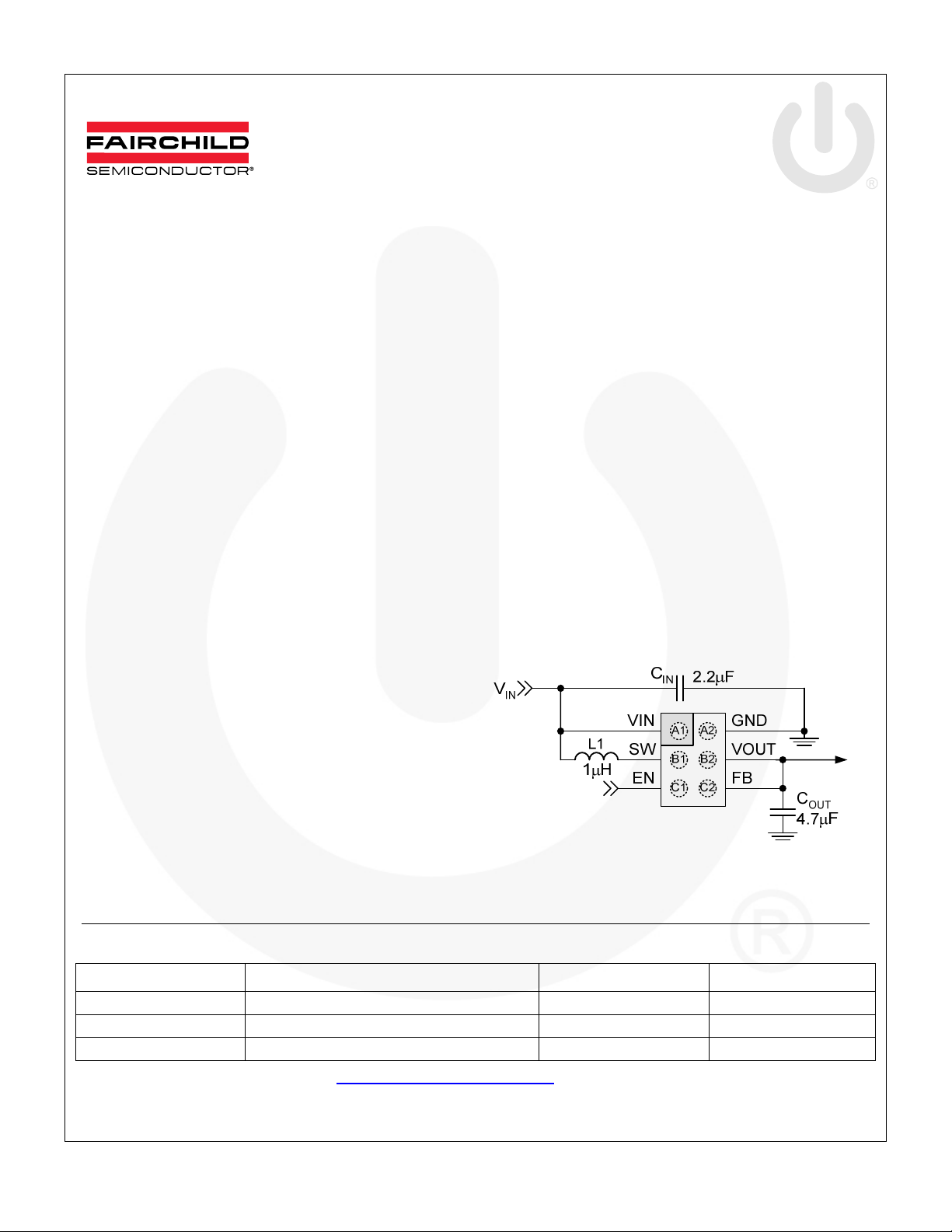
Figure 1. Typical Application
Cell Phones, Smart Phones, Portable Instruments
Ordering Information
Part Number Operating Temperature Range Package Packing Method
FAN4860UC5X -40°C to 85°C WLCSP, 0.4mm Pitch Tape and Reel
FAN4860UMP5X -40°C to 85°C UMLP-6, 2 x 2mm Tape and Reel
FAN4860UC33X -40°C to 85°C WLCSP, 0.4mm Pitch Tape and Reel
Please refer to tape and reel specifications at http://www.fairchildsemi.com/packaging.
© 2010 Fairchild Semiconductor Corporation www.fairchildsemi.com
FAN4860 • Rev. 1.1.0
Block Diagrams
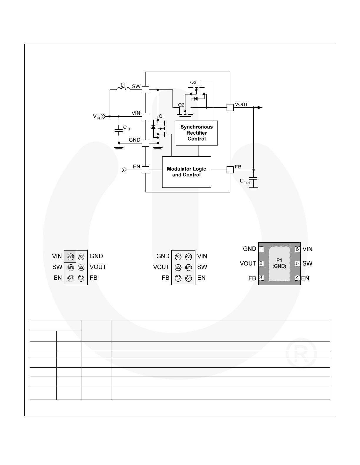
Figure 2. IC Block Diagram
FAN4860 — 3MHz, Synchronous TinyBoost™ Regulator
Pin Configuration
Figure 3. WLCSP (Top View) Figure 4. WLCSP (Bottom View) Figure 5. 2X2mm UMLP (Top View)
Pin Definitions
Pin #
WLCSP UMLP
A1 6 VIN
B1 5 SW
C1 4 EN
C2 3 FB
B2 2 VOUT
A2 1, P1 GND
Name Description
Input Voltage. Connect to Li-Ion battery input power source and input capacitor (C
Switching Node. Connect to inductor.
Enable. When this pin is HIGH, the circuit is enabled. This pin should not be left floating.
Feedback. Output voltage sense point for V
Output Voltage. This pin is both the output voltage terminal as well as an IC bias supply.
Ground. Power and signal ground reference for the IC. All voltages are measured with
respect to this pin.
. Connect to output capacitor (C
OUT
OUT
).
IN
).
© 2010 Fairchild Semiconductor Corporation www.fairchildsemi.com
FAN4860 • Rev. 1.1.0 2

FAN4860 — 3MHz, Synchronous TinyBoost™ Regulator
Absolute Maximum Ratings
Stresses exceeding the absolute maximum ratings may damage the device. The device may not function or be operable above
the recommended operating conditions and stressing the parts to these levels is not recommended. In addition, extended
exposure to stresses above the recommended operating conditions may affect device reliability. The absolute maximum
ratings are stress ratings only.
Symbol Parameter Min. Max. Units
VIN VIN Pin -0.3 5.5 V
V
VOUT Pin –2 6 V
OUT
VFB FB Pin –2 14 V
VSW SW Node
VEN EN Pin -0.3 5.5 V
ESD
TJ Junction Temperature –40 +150 °C
T
STG
TL Lead Soldering Temperature, 10 Seconds +260 °C
Electrostatic Discharge
Protection Level
Storage Temperature –65 +150 °C
DC
Transient: 10ns, 3MHz -1.0 6.5
Human Body Model per JESD22-A114 2
Charged Device Model per JESD22-C101 1
-0.3 5.5
V
kV
Recommended Operating Conditions
The Recommended Operating Conditions table defines the conditions for actual device operation. Recommended operating
conditions are specified to ensure optimal performance to the datasheet specifications. Fairchild does not recommend
exceeding them or designing to absolute maximum ratings.
Symbol Parameter Min. Max. Units
VIN Supply Voltage
I
Output Current 200 mA
OUT
TA Ambient Temperature –40 +85 °C
TJ Junction Temperature –40 +125 °C
5.0 V
3.3 V
2.3 4.5 V
OUT
2.5 3.2 V
OUT
Thermal Properties
Junction-to-ambient thermal resistance is a function of application and board layout. This data is measured with four-layer
2s2p boards in accordance to JEDEC standard JESD51. Special attention must be paid not to exceed junction temperature
at a given ambient temperate TA.
T
J(max)
Symbol Parameter Typical Units
θJA
Junction-to-Ambient Thermal Resistance
WLCSP 130 °C/W
UMLP 57 °C/W
© 2010 Fairchild Semiconductor Corporation www.fairchildsemi.com
FAN4860 • Rev. 1.1.0 3
FAN4860 — 3MHz, Synchronous TinyBoost™ Regulator
Electrical Specifications
Minimum and maximum values are at VIN=VEN=2.3V to 4.5V (2.5 to 3.2 VIN for 3.3 V
Figure 1, unless otherwise noted. Typical values are at T
=25°C, VIN=VEN=3.6V for V
A
Symbol Parameter Conditions Min. Typ. Max. Units
5.0 V
OUT
IIN VIN Input Current
3.3 V
OUT
I
V
LK_OUT
I
LK_RVSR
V
Under-Voltage Lockout VIN Rising 2.2 2.3 V
UVLO
V
UVLO_HYS
V
Enable HIGH Voltage 1.05 V
ENH
V
Enable LOW Voltage 0.4 V
ENL
I
Enable Input Leakage Current 0.01 1
LK_EN
Leakage Current V
OUT
V
to VIN Reverse Leakage
OUT
Under-Voltage Lockout Hysteresis 190 mV
Quiescent: V
Shutdown: EN=0, VIN=3.6V 0.5 1.5
Quiescent: V
Shutdown: EN=0, VIN=2.7V 0.5 1.5
=0, EN=0, VIN≥3V 10 nA
OUT
V
=5V, VIN=3.6V, EN=0
OUT
V
=3.3V, VIN=3V, EN=0
OUT
VIN from 2.3V to 4.5V, I
(1)
VIN from 2.7V to 4.5V, I
VIN from 3.3V to 4.5V, I
(1)
VIN from 2.5V to 3.2V, I
Referred to V
Referred to V
=3.6V, V
V
IN
VIN=2.7V, V
V
=2.3V 200
IN
OUT
VIN=3.3V 300
VIN=3.6V 400
V
=2.5V 250
IN
OUT
OUT
OUT
OUT
OUT
OUT
OUT
VIN=2.7V 300
VIN=3.6V, V
VIN=2.7V, V
VIN=3.6V, V
VIN=2.7V, V
VIN=3.6V, I
VIN=2.7V, I
=3.6V 300
IN
=10mA 150 °C
LOAD
OUT
5.0 V
V
3.3 V
V
Reference Accuracy
REF
t
Off Time
OFF
I
OUT
Maximum Output
Current
Output Voltage Accuracy
OUT
Output Voltage Accuracy
OUT
(2)
ISW SW Peak Current Limit
ISS
tSS Soft-Start Time
R
DS(ON)
T
T
TSD_HYS
Soft-Start Input Peak
Current Limit
N-Channel Boost Switch V
P-Channel Sync Rectifier VIN=3.6V 400
Thermal Shutdown I
TSD
(2)
(3)
Thermal Shutdown Hysteresis 30 °C
5.0 V
3.3 V
5.0 V
3.3 V
5.0 V
3.3 V
5.0 V
3.3 V
=3.6V, I
IN
=2.7V, I
IN
=5V 4.975 5.050 5.125
OUT
=3.3V 3.280 3.330 3.380
OUT
=5V, I
OUT
=3.3V, I
OUT
OUT>VIN
OUT>VIN
< VIN 850
OUT
< VIN 700
OUT
=200mA 100 300
OUT
=200mA 250 750
OUT
=0, EN=V
OUT
=0, EN=V
OUT
≤200mA 4.80 5.05 5.15
OUT
≤200mA 4.85 5.05 5.15
OUT
≤300mA 4.85 5.05 5.15
OUT
≤200mA 3.17 3.33 3.41
OUT
=200mA 195 240 265
OUT
=200mA 240 290 350
OUT
930 1100 1320
650 800 950
Notes:
1. I
from 0 to I
LOAD
; also includes load transient response. V
OUT
Effective capacitance of C
> 1.5μF.
OUT
measured from mid-point of output voltage ripple.
OUT
2. Guaranteed by design and characterization; not tested in production.
3. Elapsed time from rising EN until regulated V
OUT.
option), TA=-40°C to +85°C; circuit of
OUT
=5V, and VIN=VEN=2.7V for V
OUT
37 45
IN
50 65
IN
OUT
2.5
=3.3V.
μA
μA
μA
V
V
ns
mA
mA
mA
μs
mΩ
© 2010 Fairchild Semiconductor Corporation www.fairchildsemi.com
FAN4860 • Rev. 1.1.0 4
FAN4860 — 3MHz, Synchronous TinyBoost™ Regulator
5.0 V
Typical Characteristics
OUT
Unless otherwise specified, circuit per Figure 1, 3.6VIN, TA=25°C.
100
95
90
85
Efficiency (%)
80
75
0 50 100 150 200 250 300
Load Current (mA)
2.5 Vin
3.3 Vin
3.6 Vin
4.5 Vin
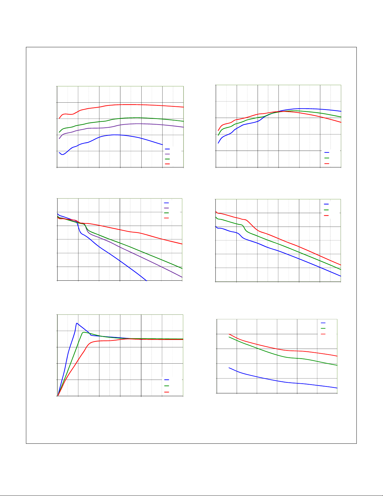
Figure 6. Efficiency vs. VIN Figure 7. Efficiency vs. Temperature, 3.6VIN
50
25
0
-25
2.5 Vin
3.3 Vin
3.6 Vin
4.5 Vin
95
92
89
Efficiency (%)
86
83
80
0 50 100 150 200 250 300
Load Current (mA)
50
25
0
-25
-40C
+25C
+85C
-40C
+25C
+85C
-50
VOUT - 5.05V (mV)
-75
-100
0 50 100 150 200 250 300
Load Current (mA)
Figure 8. Line and Load Regulation Figure 9. Load Regulation vs. Temperature, 3.6V
4000
3200
2400
1600
Frequency (KHz)
800
0
0 50 100 150 200 250 300
Load Current (mA)
Figure 10. Switching Frequency Figure 11. Quiescent Current
2.5 Vin
3.6 Vin
4.5 Vin
-50
VOUT - 5.05V (mV)
-75
-100
0 50 100 150 200 250 300
Load Current (mA)
IN
50
45
40
35
Quiescent Current (uA)
30
25
2.0 2.5 3.0 3.5 4.0 4.5 5.0
Input Voltage(V)
-40C
+25C
+85C
© 2010 Fairchild Semiconductor Corporation www.fairchildsemi.com
FAN4860 • Rev. 1.1.0 5
FAN4860 — 3MHz, Synchronous TinyBoost™ Regulator
5.0 V
Unless otherwise specified, circuit per Figure 1, 3.6VIN, TA=25°C.
Typical Characteristics
OUT
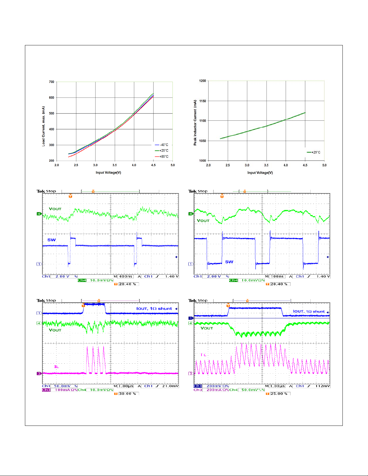
Figure 12. Maximum DC Load Current Figure 13. Peak Inductor Current
Figure 14. Output Ripple, 10mA PFM Load Figure 15. Output Ripple, 200mA PWM Load
Figure 16. 0-50mA Load Transient, 100ns Step Figure 17. 50-200mA Load Transient, 100ns Step
© 2010 Fairchild Semiconductor Corporation www.fairchildsemi.com
FAN4860 • Rev. 1.1.0 6
 Loading...