

查询DM7490A供应商
DM7490A
Decade and Binary Counters
DM7490A Decade and Binary Counters
August 1986
Revised March 2000
General Description
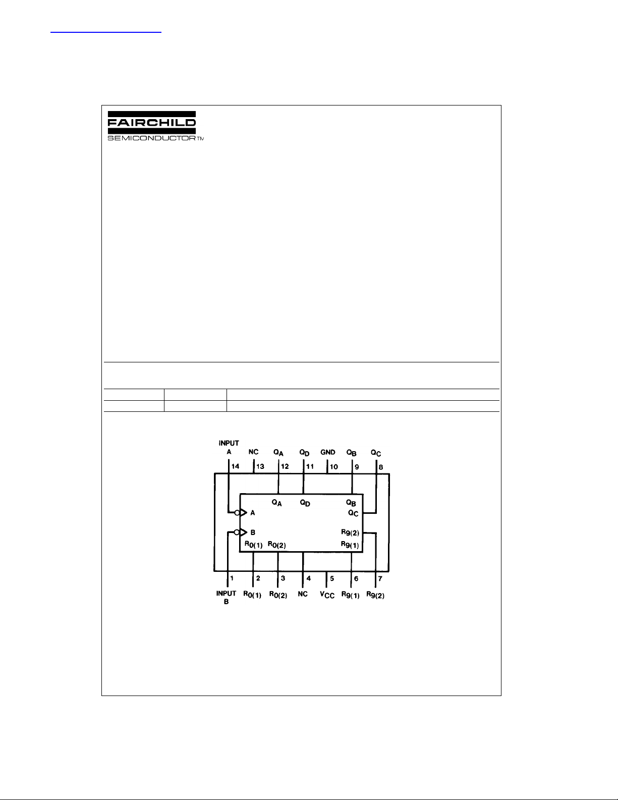
The DM7490A monolithic counter contains four masterslave flip-flops and additio nal ga ting to pr ovi d e a divid e-b ytwo counter and a three-stage binary counter for which the
count cycle length is divide-by-five.
The counter has a gated zero reset and also has gated setto-nine inputs for use in BCD nine’s complement applications.
To use the maximum count length (decade or four-bit
binary), the B input is connected to the Q
input count pulses are applied to input A and the outputs
are as described in the app rop ria te F un c tion Table. A symmetrical divide-by-ten count can be obtained from the
counters by connecting the Q
applying the input count to the B input which gives a divideby-ten square wave at output Q
output to the A input and
D
.
A
output. The
A
Features
■ Typical power dissipation
145 mW
■ Count frequency 42 MHz
Ordering Code:
Order Number Package Number Package Description
DM7490AN N14A 14-Lead Plastic Dual-In-Line Package (PDIP), JEDEC MS-001, 0.300 Wide
Connection Diagram
© 2000 Fairchild Semiconductor Corporation DS006533 www.fairchildsemi.com
Function Tables
BCD Count Sequence (Note 1)
Count Outputs
DM7490A
0 LLLL
1LLLH
2LLHL
3LLHH
4LHLL
5LHLH
6LHHL
7LHHH
8 HLLL
9HLLH
Count Outputs
0 LLLL
1LLLH
2LLHL
3LLHH
4LHLL
5 HLLL
6HLLH
7HLHL
8HLHH
9HHLL
Q
D
BCD Bi-Quinary (5-2) (Note 2)
Q
A
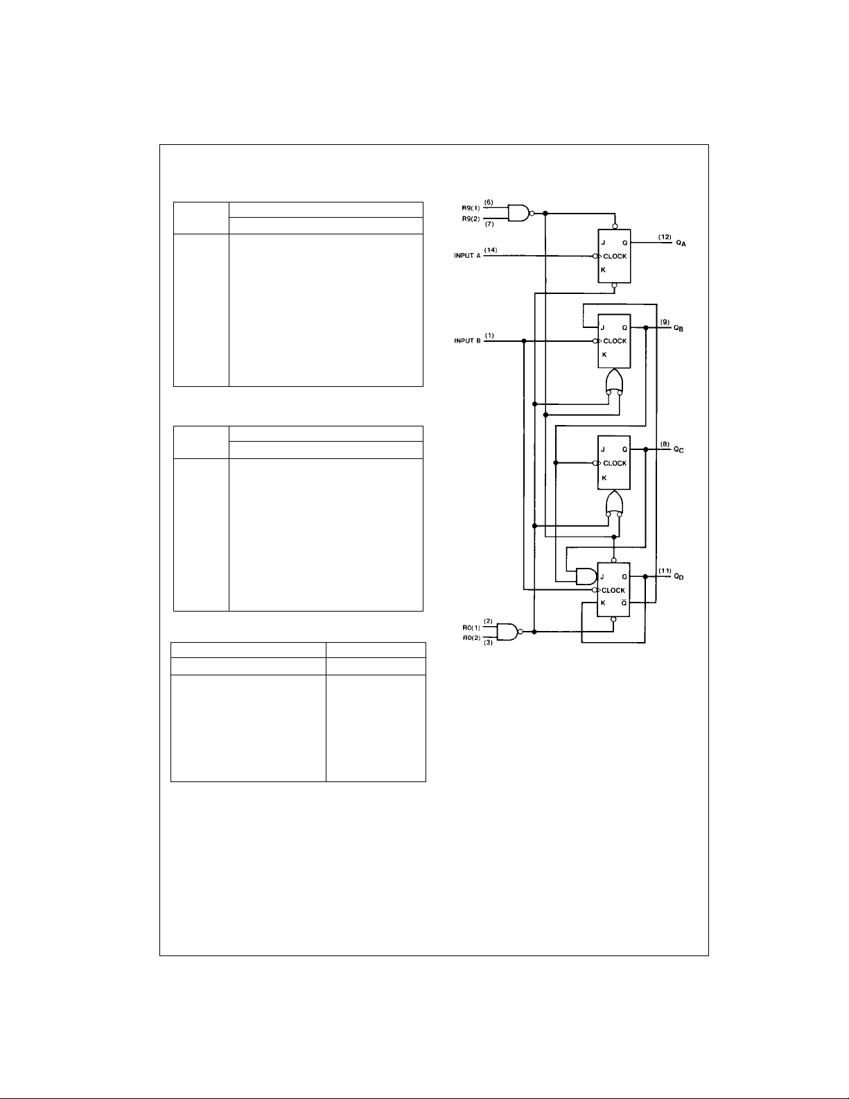
Logic Diagram
Q
C
Q
D
Q
Q
Q
B
C
A
Q
B
Reset/Count Function Table
Reset Inputs Outputs
R0(1) R0(2) R9(1) R9(2) Q
DQCQBQA
H H L X LLLL
H H X L LLLL
XXHHHLLH
X L X L COUNT
L X L X COUNT
L X X L COUNT
X L L X COUNT
H = HIGH Level
L = LOW Level
X = Don’t Care
Note 1: Output QA is connected to input B for BCD count.
Note 2: Output QD is c onnected to input A for bi- quinary count
www.fairchildsemi.com 2
The J and K inputs sho wn without connec tion are for refere nce only and
are functionally at a H IG H lev el.

Absolute Maximum Ratings(Note 3)
Supply Voltage 7V
Input Voltage 5.5V
Operating Free Air Temperature Range 0°C to +70°C
Storage Temperature Range −65°C to +150°C
Note 3: The “Absolute Maximum Ratings ” are those val ues beyond w hich
the safety of the device cannot be guaranteed. The device should not be
operated at these limits. The parametric values defined in the Electrical
Characteristics tables are not guaranteed at the absolute maximum ratings.
The “Recommend ed O peratin g Cond itions” t able w ill defin e the condit ions
for actual device operation.
Recommended Operating Conditions
Symbol Parameter Min Nom M ax Units
V
V
V
I
I
f
CC
IH
IL
OH
OL
CLK
Supply Voltage 4.75 5 5.25 V
HIGH Level Input Voltage 2 V
LOW Level Input Voltage 0.8 V
HIGH Level Output Current −0.8 mA
LOW Level Output Current 16 mA
Clock Frequency A 0 32
(Note 4) B 0 16
t
W
Pulse Width A 15
(Note 4) B 30 ns
Reset 15
t
REL
T
A
Note 4: TA = 25°C and VCC = 5V.
Reset Release Time (Note 4) 25 ns
Free Air Operating Temperature 0 70 °C
DC Electrical Characteristics
over recommended operating free air temperature range (unless otherwise noted)
Symbol Parameter Conditions Min
V
I
V
OH
V
OL
I
I
I
IH
I
IL
I
OS
I
CC
Note 5: All typicals are at VCC = 5V, TA = 25°C.
Note 6: Q
Note 7: Not more than one output should be shorted at a time.
Note 8: I
Input Clamp Voltage VCC = Min, II = −12 mA −1.5 V
HIGH Level VCC = Min, IOH = Max
Output Voltage VIL = Max, VIH = Min
LOW Level VCC = Min, IOL = Max
Output Voltage VIH = Min, VIL = Max (Note 6)
Input Current @ Max Input V o ltage VCC = Max, VI = 5.5V 1 mA
HIGH Level VCC = Max A 80
Input Current VI = 2.7V Reset 40 µA
LOW Level VCC = Max A −3.2
Input Current VI = 0.4V Reset −1.6 mA
Short Circuit Output Current VCC = Max (Note 7) −18 −57 mA
Supply Current VCC = Max (Note 8) 29 42 mA
outputs are tested at IOL = Max plus the limit value of IIL for the B input. This per m it s driv ing the B input while maintaining full fan-out c apability.
A
is measured with all out puts open, both RO inp ut s grounded following m om entary connection to 4.5 V, and all other inputs grounded.
CC
B 120
B −4.8
2.4 3.4 V
Typ
(Note 5)
0.2 0.4 V
Max Units
DM7490A
MHz
3 www.fairchildsemi.com

AC Switching Characteristics
at VCC = 5V and TA = 25°C
Symbol Parameter
DM7490A
f
t
t
t
t
t
t
t
t
t
t
t
t
t
MAX
PLH
PHL
PLH
PHL
PLH
PHL
PLH
PHL
PLH
PHL
PLH
PHL
PHL
Maximum Clock A to Q
Frequency B to Q
Propagation Delay Time
LOW-to-HIGH Level Output
Propagation Delay Time
HIGH-to-LOW Level Output
Propagation Delay Time
LOW-to-HIGH Level Output
Propagation Delay Time
HIGH-to-LOW Level Output
Propagation Delay Time
LOW-to-HIGH Level Output
Propagation Delay Time
HIGH-to-LOW Level Output
Propagation Delay Time
LOW-to-HIGH Level Output
Propagation Delay Time
HIGH-to-LOW Level Output
Propagation Delay Time
LOW-to-HIGH Level Output
Propagation Delay Time
HIGH-to-LOW Level Output
Propagation Delay Time
LOW-to-HIGH Level Output
Propagation Delay Time
HIGH-to-LOW Level Output
Propagation Delay Time SET-0
HIGH-to-LOW Level Output Any Q
From (Input)
RL = 400Ω, CL = 15 pF
To (Output) Min Max
A
B
A to Q
A
A to Q
A
A to Q
D
A to Q
D
B to Q
B
B to Q
B
B to Q
C
B to Q
C
B to Q
D
B to Q
D
SET-9 to QA, Q
SET-9 to QB, Q
D
C
32
16
Units
MHz
16 ns
18 ns
48 ns
50 ns
16 ns
21 ns
32 ns
35 ns
32 ns
35 ns
30 ns
40 ns
40 ns
www.fairchildsemi.com 4

Physical Dimensions inches (millimeters) unless otherwise noted
DM7490A Decade and Binary Counters
14-Lead Plastic Dual-In-Line Package (PDIP), JEDEC MS-001, 0.300 Wide
Fairchild does not assume any responsibility for use of any circuitry described, no circuit patent license s are implied and
Fairchild reserves the right at any time without notice to change said circuitry and specifications.
LIFE SUPPORT POLICY
FAIRCHILD’S PRODUCTS ARE NOT AUTHORIZED FOR USE AS CRITICAL COMPONENTS IN LIFE SUPPORT
DEVICES OR SYSTEMS WITHOUT THE EXPRESS WRITTEN APPROVAL OF THE PRESIDENT OF FAIRCHILD
SEMICONDUCTOR CORPORATION. As used herein:
1. Life support devices or syst ems are dev ices or syste ms
which, (a) are intended for surgical implant into the
body, or (b) support or sustain life, and (c) whose failure
to perform when properly used in accordance with
instructions for use provide d in the labe l ing, can be re asonably expected to result in a significant injury to the
user.
Package Number N14A
2. A critical compo nent in any com ponen t of a life s uppor t
device or system whose failu re to perform can b e reasonably expected to cause the failure of the life support
device or system, or to affect its safety or effectiveness.
www.fairchildsemi.com
5 www.fairchildsemi.com
 Loading...