

Page 1
DM7446A, DM7447A
BCD to 7-Segment Decoders/Drivers
DM7446A, DM7447A BCD to 7-Segment Decoders/Drivers
September 1986
Revised February 2000
General Description
The DM7446A and DM74 47A feature active- LOW outputs
designed for driving common- ano de LEDs or inc and esce nt
indicators directly. All of the circuits have full ripple-blanking input/output controls and a lamp test input. Segment
identification and resu ltant di splays a re shown on a fo llowing page. Display patterns for BCD input counts above nine
are unique symbols to authenticate input conditions.
All of the circuits incorporate automatic leading and/or trailing-edge, zero-blankin g control (RBI and RBO). Lam p test
(LT) of these devices may be performed at any time when
the BI/RBO node is at a HIGH logic level. All typ es cont ain
an overriding blanking input (BI) which can be used to control the lamp intensity (by pulsing) or to inhibit the outputs.
Features
■ All circuit types featur e lamp inte nsity modulati on capability
■ Open-collector outputs drive indicators directly
■ Lamp-test provision
■ Leading/trailing zero suppression
Ordering Code:
Order Number Package Number Package Description
DM7446AN N16E 16-Lead Plastic Dual-In-Line Package (PDIP), JEDEC MS-001, 0.300 Wide
DM7446AN N16E 16-Lead Plastic Dual-In-Line Package (PDIP), JEDEC MS-001, 0.300 Wide
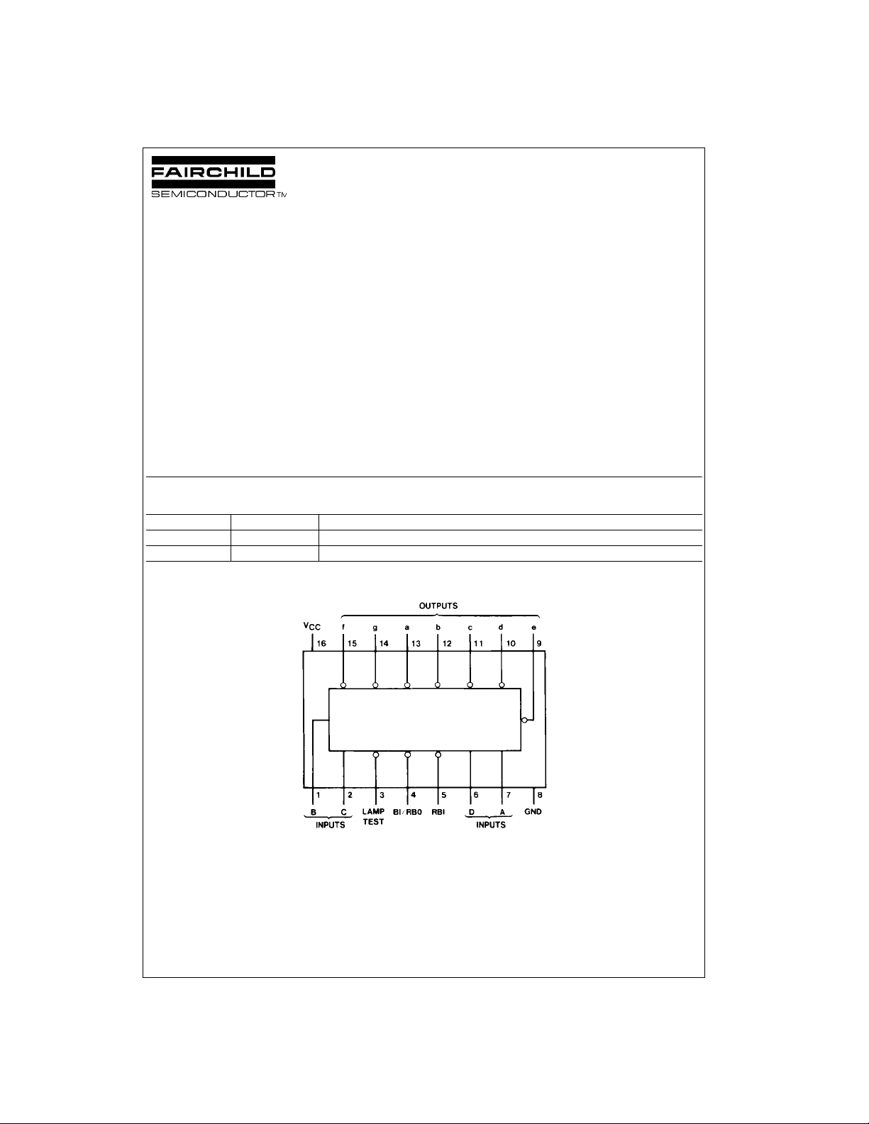
Connection Diagram
© 2000 Fairchild Semiconductor Corporation DS006518 www.fairchildsemi.com
Page 2
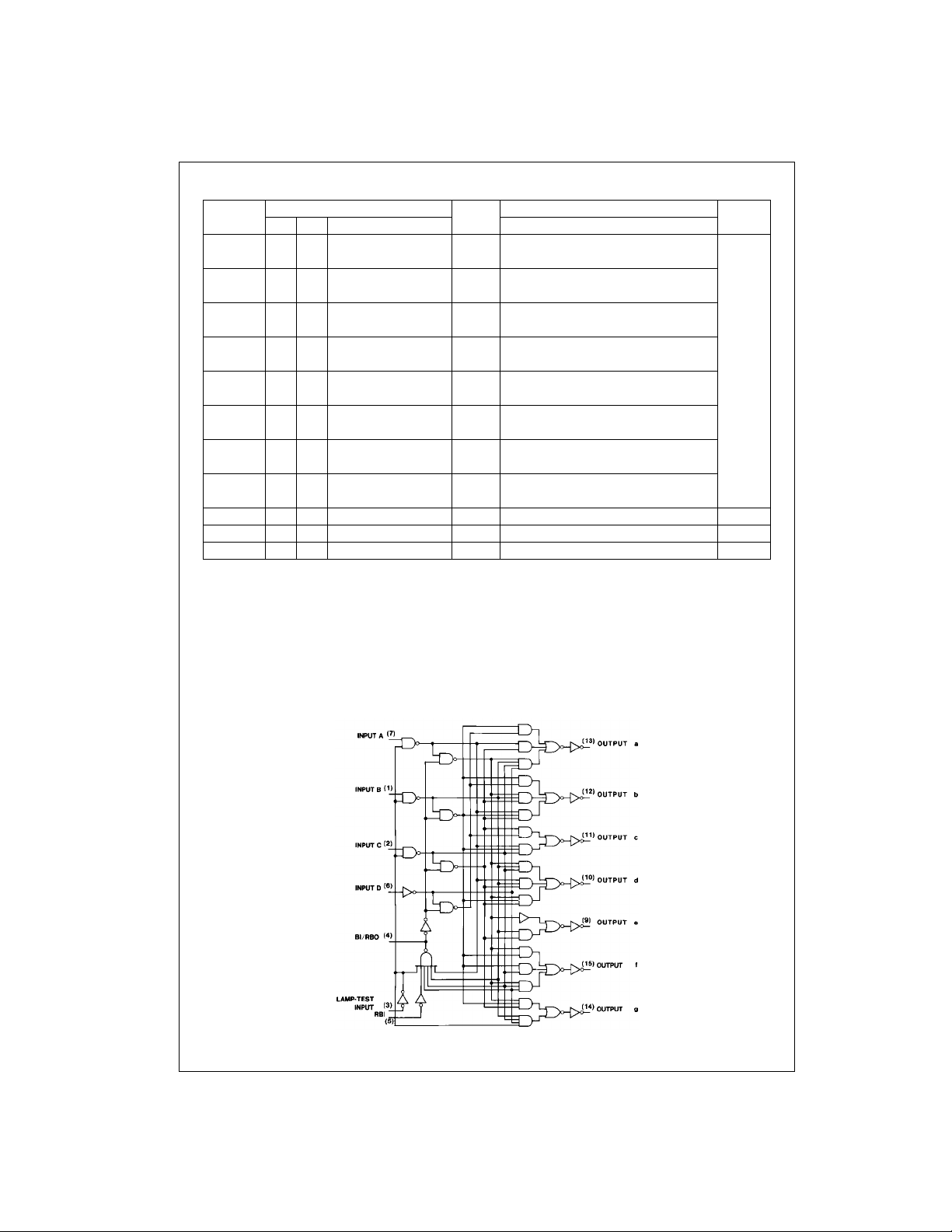
Function Table
Decimal or Inputs BI/RBO Outputs
Function LT RBI D C B A (Note 1) a b c d e f g
0 HHLLLL H LLLLLLH
1 HXLLLH H HLLHHHH
2 HXLLHL H LLHLLHL
3 HXLLHH H LLLLHHL
DM7446A, DM7447A
4 HXLHLL H HLLHHLL
5 HXLHLH H LHLLHLL
6 HXLHHL H HHLLLLL
7 HXLHHH H L LLHHHH(Note 2)
8 HXHLLL H LLLLLLL
9 HXHLLH H LLLHHLL
10 HXHLHL H HHHLLHL
11 HXHLHH H HHLL HHL
12 HXHHL L H HLHHHL L
13 HXHHLH H LHHLHLL
14 HXHHHL H HHHLLLL
15 HXHHHH H HHHHHHH
BI XXXXXX L HHHHHHH(Note 3)
RBI HLL LLL L HHHHHHH(Note 4)
LT LXXXXX H LLLLLLL(Note 5)
H = HIGH level, L = LOW level, X = Don’t Care
Note 1: BI/RBO is a wire-AND logic servin g as blanking input (BI) and / or ripple-blanking outp ut ( R BO).
Note 2: The blanking input (BI) must be OPEN o r held at a HIGH logic le v el w hen output functions 0 t hrough 15 are desir ed. The ripple-blanking input (RBI)
must be OPEN or HI GH if blanking of a decimal ze ro is not desired.
Note 3: When a LOW logic level is applied dire c t ly to the blanking input (BI), all segment outputs are HIGH regardless of the level of any other input.
Note 4: When ripple-blanking input (RBI) and inputs A, B, C , and D are at a LOW level with the lamp test input HI GH , all segment outputs go H and the rip-
ple-blanking output (RBO) goes to a LOW level (response condition).
Note 5: When the blanking input/ripple-blanking output (BI/RBO) is OPEN or held HIGH and a LOW is applied to the lamp-test input, all segment outputs are
L.
Note
Logic Diagram
www.fairchildsemi.com 2
Page 3
Absolute Maximum Ratings(Note 6)
Supply Voltage 7V
Input Voltage 5.5V
Operating Free Air Temperature Range 0°C to +70°C
Storage Temperature Range −65°C to +150°C
Note 6: The “Absolute M aximu m R atin gs” are t hose valu es b eyo nd w hich
the safety of the device cannot be guaranteed. The device should not be
operated at these limits. The parametric values defined in the Electrical
Characteristics tables are not guaranteed at the absolute maximum ratings.
The “Recommend ed O peratin g Cond itions” t able w ill defin e the condit ions
for actual device operation.
Recommended Operating Conditions
Symbol Parameter Min Nom Max Units
DM7446A
V
CC
V
IH
V
IL
V
OH
I
OH
I
OL
I
OL
T
A
DM7447A
V
CC
V
IH
V
IL
V
OH
I
OH
I
OL
I
OL
T
A
Supply Voltage 4.75 5 5.25 V
HIGH Level Input Voltage 2 V
LOW Level Input Voltage 0.8 V
HIGH Level Output Voltage (a thru g) 30 V
HIGH Level Output Current (BI/RBO) −0.2 µA
LOW Level Output Current (a thru g) 40 mA
LOW Level Output Current (BI/RBO) 8 mA
Free Air Operating Temperature 0 70 °C
Supply Voltage 4.75 5 5.25 V
HIGH Level Input Voltage 2 V
LOW Level Input Voltage 0.8 V
HIGH Level Output Voltage (a thru g) 15 V
HIGH Level Output Current (BI/RBO) −0.2 µA
LOW Level Output Current (a thru g) 40 mA
LOW Level Output Current (BI/RBO) 8 mA
Free Air Operating Temperature 0 70 °C
DM7446A, DM7447A
3 www.fairchildsemi.com
Page 4
DM7446A Electrical Characteristics
over recommended operating free air temperature range (unless otherwise noted)
Symbol Parameter Conditions Min
V
I
V
OH
Input Clamp Voltage VCC = Min, II = −12 mA −1.5 V
HIGH Level Output VCC = Min
Voltage (BI/RBO) IOH = Max
I
CEX
HIGH Level Output VCC = Max, VO = 30V
Current (a thru g) VIL = Max, VIH = Min
DM7446A, DM7447A
V
OL
LOW Level VCC = Min, IOL = Max
Output Voltage VIH = Min, VIL = Max
I
I
Input Current @ Max VCC = Max, VI = 5.5V
Input Voltage (Except BI/RBO)
I
IH
HIGH Level Input VCC = Max, VI = 2.4V
Current (Except BI/RBO)
I
IL
LOW Level Input VCC = Max BI/RBO −4
Current VI = 0.4V Others −1.6
I
OS
Short Circuit VCC = Max
Output Current (BI/RBO)
I
CC
Supply Current VCC = Max
(Note 8)
Note 7: All typicals are at VCC = 5V, TA = 25°C.
Note 8: I
is measured with all out puts OPEN and all inpu ts at 4.5V.
CC
Typ
(Note 7)
Max Units
2.4 3.7 V
250 µA
0.3 0.4 V
1mA
40 µA
−4mA
60 103 mA
DM7446A Switching Characteristics
at VCC = 5V and TA = 25°C
Symbol Parameter Conditions Min Max Units
t
PLH
t
PHL
Propagation Delay Time CL = 15 pF
LOW-to-HIGH Level Output RL = 120Ω
Propagation Delay Time
HIGH-to-LOW Level Output
100 ns
100 ns
mA
www.fairchildsemi.com 4
Page 5
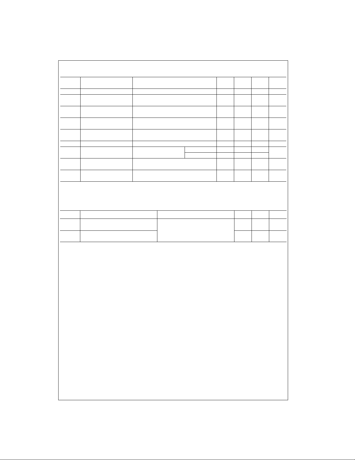
DM7447A Electrical Characteristics
over recommended operating free air temperature range (unless otherwise noted)
Symbol Parameter Conditions Min
V
I
V
OH
Input Clamp Voltage VCC = Min, II = −12 mA −1.5 V
HIGH Level Output VCC = Min
Voltage (BI/RBO) IOH = Max
I
CEX
HIGH Level Output VCC = Max, VO = 15V
Current (a thru g) VIL = Max, VIH = Min
V
OL
LOW Level Output VCC = Min, IOL = Max
Voltage VIH = Min, VIL = Max
I
I
Input Current @ Max VCC = Max, VI = 5.5V 1 mA
Input Voltage
I
IH
I
IL
HIGH Level Input Current VCC = Max, VI = 2.4V 40 µA
LOW Level Input VCC = Max BI/RBO −4
Current VI = 0.4V Others −1.6
I
OS
Short Circuit VCC = Max
Output Current (BI/RBO)
I
CC
Supply Current VCC = Max
(Note 10)
Note 9: All typicals are at VCC = 5V, TA = 25°C.
Note 10: I
is measured with all out put s OPEN and all inputs at 4. 5V.
CC
Typ
(Note 9)
Max Units
2.4 3.7 V
250 µA
0.3 0.4 V
−4mA
60 103 mA
DM7447A Switching Characteristics
at VCC = 5V and TA = 25°C
Symbol Parameter Conditions Min Max Units
t
PLH
t
PHL
Propagation Delay Time CL = 15 pF
LOW-to-HIGH Level Output RL = 120Ω
Propagation Delay Time
HIGH-to-LOW Level Output
100 ns
100 ns
DM7446A, DM7447A
mA
5 www.fairchildsemi.com
Page 6
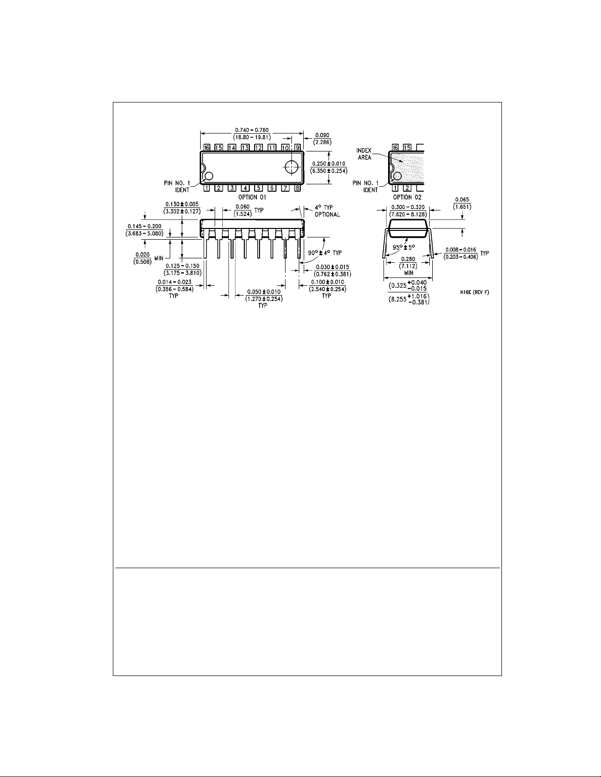
Physical Dimensions inches (millimeters) unless otherwise noted
16-Lead Plastic Dual-In-Line Package (PDIP), JEDEC MS-001, 0.300 Wide
Package Number N16E
DM7446A, DM7447A BCD to 7-Segment Decoders/Drivers
Fairchild does not assume any responsibility for us e of any circuitry described, no circuit patent licenses are implied and
Fairchild reserves the right at any time without notice to change said circuitry and specifications.
LIFE SUPPORT POLICY
FAIRCHILD’S PRODUCTS ARE NOT AUTHORIZED FOR USE AS CRITICAL COMPONENTS IN LIFE SUPPORT
DEVICES OR SYSTEMS WITHOUT THE EXPRESS WRITTEN APPROVAL OF THE PRESIDENT OF FAIRCHILD
SEMICONDUCTOR CORPORATION. As used herein:
1. Life supp or t de vices o r syste ms are device s or syste ms
which, (a) are intended for surgical implant into the
body, or (b) support or sustain life, and (c) whose failure
to perform when properly used in accordance with
instructions for use provided in the labeling, can be reasonably expected to result in a significan t injury to the
user.
2. A cr itical compon ent i n any compon ent of a life su pport
device or system whose failu re to perform can be reasonably expected to ca use the fa i lure of the li fe su pp ort
device or system, or to affect its safety or effectiveness.
www.fairchildsemi.com
www.fairchildsemi.com 6
 Loading...