

December 2010
BSS138W
N-Channel Logic Level Enhancement Mode Field Effect Transistor
BSS138W — N-Channel Logic Level Enhancement Mode Field Effect Transistor
General Description
These N-Channel enhancement mode field effect
transistor. These products have been designed to
minimize on-state resistance while provide rugged,
reliable, and fast switching performance.These products are particularly suited for low voltage, low current
applications such as small servo motor control, power
MOSFET gate drivers, and other switching applications.
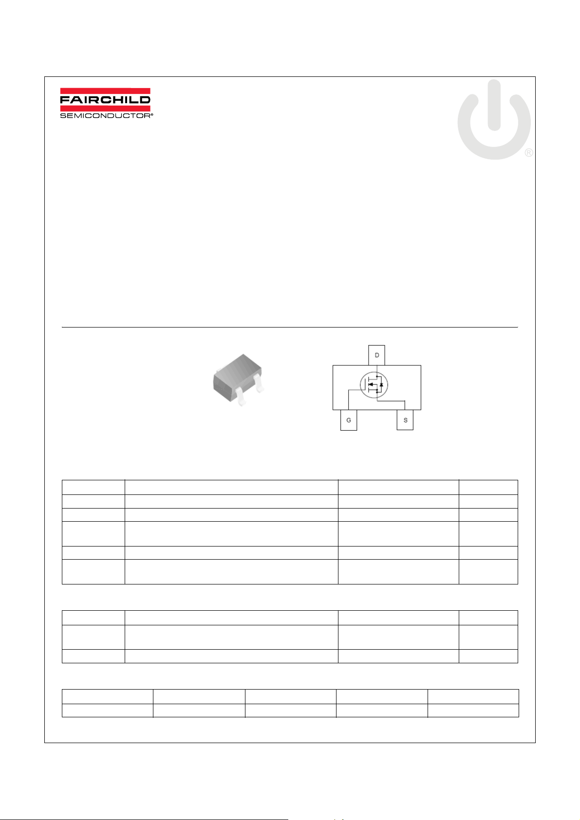
D
G
SOT-323
Marking : 138
Absolute Maximum Ratings T
= 25°C unless otherwise noted
A
S
Features
•R
R
• High density cell design for extremely low R
• Rugged and Reliable
• Compact industry standard SOT-323 surface mount
package
= 3.5Ω @ VGS = 10V, ID = 0.22A
DS(ON)
= 6.0Ω @ VGS = 4.5V, ID = 0.22A
DS(ON)
Symbol Parameter Value Units
V
DSS
V
GSS
I
Drain Current - Continuous (Note1)
D
T
J, TSTG
T
L
Drain-Source Voltage 50 V
Gate-Source Voltage ±20 V
0.21
- Pulsed
Operating and Storage Junction Temperature Range -55 to +150 °C
Maximum Lead Temperature for Soldering
Purposes, 1/16” from Case for 10 Seconds
0.84
300 °C
DS(ON)
A
A
Thermal Characteristics
Symbol Parameter Value Units
P
D
R
θJA
Maximum Power Dissipation (Note1)
Derate Above 25°C
Thermal Resistance, Junction to Ambient (Note1) 367 °C/W
340
2.72
mW
mW/°C
Package Marking and Ordering Information
Device Marking Device Reel Size Tape width Quantity
138 BSS138W 7’’ 8mm 3000 units
© 2010 Fairchild Semiconductor Corporation www.fairchildsemi.com
BSS138W Rev. A0 1
BSS138W — N-Channel Logic Level Enhancement Mode Field Effect Transistor
Electrical Characteristics T
= 25°C unless otherwise noted
A
Symbol Parameter Test Condition Min. Typ. Max. Units
Off Characteristics
BV
ΔBV
ΔT
I
I
DSS
DSS
GSS
Drain-Source Breakdown Voltage V
Breakdown Voltage Temperature
DSS
Coefficient
J
Zero Gate Voltage Drain Current V
Gate-Body Leakage V
= 0V, ID = 250μA50 V
GS
ID = 250μA, Referenced to 25°C71mV/°C
DS
V
DS
V
DS
GS
= 50V, V
= 50V, V
= 30V, V
= ±20V, V
= 0V
GS
= 0V, TJ = 125°C
GS
= 0V
GS
= 0V ±100 nA
DS
0.5
5
100
On Characteristics (Note2)
V
ΔV
R
I
GS(th)
GS(th)
ΔT
DS(ON)
D(ON)
g
FS
Gate Threshold Voltage VDS = VGS, ID = 1mA 0.8 1.3 1.5 V
Gate Threshold Voltage
Temperature Coefficient
J
Static Drain-Source
On-Resistance
On-State Drain Current V
ID = 1mA, Referenced to 25°C-3.9mV/°C
VGS = 10V, ID = 0.22A
= 4.5V, ID = 0.22A
V
GS
VGS = 10V , ID = 0.22A, TJ=125°C
= 10V, V
GS
= 5V 0.2 A
DS
1.17
1.36
2.16
Forward Transconductance VDS = 10V, ID = 0.22A 0.12 S
3.5
6.0
5.8
Dynamic Characteristics
C
C
oss
C
rss
R
Input Capacitance
iss
V
Output Capacitance 5.9 pF
= 25V , V
DS
= 0V , f = 1.0MHz
GS
38 pF
Reverse Transfer Capacitance 3.5 pF
Gate Resistance V
G
= 15mV, f = 1.0MHz 11 Ω
GS
Switching Characteristics (Note2)
t
d(on)
t
t
d(off)
Q
Q
Q
t
Turn-On Delay Time
Turn-On Rise Time 1.9 18
r
Turn-Off Delay Time 6.7 36
Turn-Off Fall Time 6.5 14
f
Total Gate Change
g
Gate-Source Change 0.12
gs
Gate-Drain Change 0.22
gd
VDD = 30V, ID = 0.29A,
V
= 10V, R
GS
= 25V, ID = 0.22A,
V
DS
= 10V
V
GS
GEN
= 6Ω
2.3 5 ns
1.1 nC
Drain-Source Diode Characteristics and Maximum Ratings
I
V
SD
Notes:
1. 367°C/W when mounted on a minimum pad.
2. Pulse Test: Pulse Width ≤ 300μs, Duty Cycle ≤ 2.0%
Maximum Continuous Drain–Source Diode Forward Current 0.22 A
S
Drain-Source Diode Forward
VGS = 0V, IS = 0.44A (Note2) 1.4 V
Voltage
μA
μA
nA
Ω
Ω
Ω
ns
ns
ns
nC
nC
© 2010 Fairchild Semiconductor Corporation www.fairchildsemi.com
BSS138W Rev. A0 2

Typical Performance Characteristics
BSS138W — N-Channel Logic Level Enhancement Mode Field Effect Transistor
Figure 1. On-Region Characteristics. Figure 2. On-Resistance Variation with
2.0
1.5
6V
4.5V
1.0
. Drain-Source Current (A)
0.5
D
I
0.0
0.0 0.5 1.0 1.5 2.0 2.5 3.0
3.5V
VDS. Drain-Source Voltage (V)
Figure 3. On-Resistance Variation with
Temperature.
2.5
VGS = 10V
I
= 220 mA
D
2.0
(Ω)
1.5
(on)
DS
R
1.0
Normalized Drain-Source On-Resistance
0.5
-50 0 50 100 150
TJ. Junction Temperature (oC)
VGS = 10V
3V
2.5V
2V
Drain Current and Gate Voltage.
3.5
3.0
2.5
(Ω)
3V
(on),
DS
R
VGS = 2.5V
2.0
1.5
Drain-Source On-Resistance
1.0
0.5
0.00.20.40.60.81.0
3.5V
4.5V
4V
10V
6V
ID. Drain-Source Current(A)
Figure 4. On-Resistance Variation with
Gate-to-Source Voltage.
4.0
3.5
3.0
2.5
(Ω)
2.0
(on)
DS
R
1.5
1.0
Drain-Source On-Resistance
0.5
0.0
0246810
TA = 25oC
TA = 125oC
VGS. Gate to Source Voltage(V)
ID = 110 mA
Figure 5. Drain-Source On Voltage with
Temperature.
2.0
VGS = 10V
1.6
1.2
0.8
. Drain-Source On Volt age ( V )
DS
0.4
V
0.0
0.0 0.1 0.2 0.3 0.4 0.5 0.6
ID. Drain Current (A)
TA = 125(oC)
TA = 25(oC)
TA = -55(oC)
Figure 6. Body Diode Forward Voltage Variation
with Source Current and Temperature.
1000
VGS = 0 V
100
10
1
. Reverse Drain Current [mA]
S
I
0.1
0.0 0.2 0.4 0.6 0.8 1.0 1.2
TA=150oC
TA=25oC
TA=-55oC
VSD. Body Diode Forward Voltage [V]
© 2010 Fairchild Semiconductor Corporation www.fairchildsemi.com
BSS138W Rev. A0 3

Typical Performance Characteristics (Continued)
BSS138W — N-Channel Logic Level Enhancement Mode Field Effect Transistor
Figure 7. Gate Charge Characteristics.
10
ID = 220mA
8
VDS = 8V
6
4
. Gate-Source Voltage ( V )
GS
V
2
0
0.0 0.2 0.4 0.6 0.8 1.0 1.2
VDS = 30V
VDS = 25V
Qg. Gate Charg e (nC)
Figure 9. Maximum Safe Operating Area.
Limit
10
0
VGS=10V
Single Pulse
Rthja=367
T
= 25oC
a
100μs
1ms
10ms
100ms
1s
DC
o
C/W
1
10
, Drain Current [A]
D
I
1
10
0
10
-1
10
R
DS(on)
-2
10
-3
10
-1
10
VDS, Drain-Source Voltage [V]
Figure 8. Capacitance Characteristics.
100
80
60
. Capacitance (pF)
RSS
40
C
OSS,
C
ISS,
20
C
0
C
ISS
C
OSS
C
RSS
0 1020304050
VDS. Voltage Bias (V)
f = 1M H Z
V
= 0V
GS
Figure 10. Single Pulse Maximum
Power Dissipation.
5
4
3
2
1
P(pk), Peak Transient Power (W)
2
10
0
1E-3 0.01 0.1 1 10 100
t1, Time(sec)
Single Pulse
o
Rthja=367
C/W
T
=25
A
Figure 11. Transient Thermal Response Curve.
1
50%
Rthja(t)=r(t)*Rthja
30%
0.1
10%
5%
2%
D=1%
r(t), Normalized Transient Thermal Resistance
Single Pulse
0.01
1E-4 1E-3 0.01 0.1 1 10 100 1000
t1, time(sec)
© 2010 Fairchild Semiconductor Corporation www.fairchildsemi.com
BSS138W Rev. A0 4
Rthja=367
o
C/W

Physical Dimensions
BSS138W — N-Channel Logic Level Enhancement Mode Field Effect Transistor
1.25±0.10 2.10±0.10
1.00±0.10
2.00±0.20
SOT-323
0.275±0.100
0.95±0.15
0.05
3°
+0.05
–0.02
0.90
±0.10
3°
1.30±0.10
+0.04
0.135
–0.01
0.10 Min
Dimensions in Millimeters
© 2010 Fairchild Semiconductor Corporation www.fairchildsemi.com
BSS138W Rev. A0 5

TRADEMARKS
The following includes registered and unregistered trademarks and service marks, owned by Fairchild Semiconductor and/or its global subsidiaries, and is not
intended to be an exhaustive list of all such trademarks.
®
AccuPower¥
Auto-SPM¥
Build it Now¥
CorePLUS¥
CorePOWER¥
CROSSVOLT¥
CTL¥
Current Transfer Logic¥
DEUXPEED
Dual Cool™
EcoSPARK
®
®
EfficientMax¥
ESBC¥
®
®
Fairchild
Fairchild Semiconductor
FACT Quiet Series¥
®
FACT
®
FAST
FastvCore¥
FETBench¥
FlashWriter
®
*
FPS¥
F-PFS¥
®
FRFET
Global Power Resource
SM
Green FPS¥
Green FPS¥ e-Series¥
Gmax¥
GTO¥
IntelliMAX¥
ISOPLANAR¥
MegaBuck¥
MICROCOUPLER¥
MicroFET¥
MicroPak¥
MicroPak2¥
MillerDrive¥
®
MotionMax¥
Motion-SPM¥
OptoHiT™
OPTOLOGIC
OPTOPLANAR
®
®
®
PDP SPM™
Power-SPM¥
PowerTrench
®
PowerXS™
Programmable Active Droop¥
®
QFET
QS¥
Quiet Series¥
RapidConfigure¥
¥
Saving our world, 1mW/W/kW at a time™
SignalWise¥
SmartMax¥
SMART START¥
®
SPM
STEALTH¥
SuperFET
®
SuperSOT¥-3
SuperSOT¥-6
SuperSOT¥-8
SupreMOS
®
SyncFET¥
Sync-Lock™
The Power Franchise
TinyBoost¥
TinyBuck¥
TinyCalc¥
TinyLogic
TINYOPTO¥
TinyPower¥
TinyPWM¥
TinyWire¥
TriFault Detect¥
TRUECURRENT¥*
PSerDes¥
UHC
Ultra FRFET¥
UniFET¥
VCX¥
VisualMax¥
XS™
*
®
®
®
* Trademarks of System General Corporation, used under license by Fairchild Semiconductor.
DISCLAIMER
FAIRCHILD SEMI CONDUCTOR RESERVES THE RIGHT TO M AKE CHANGES WITHOUT FURTHER NOTICE TO ANY PRODUCTS HEREI N TO IMPRO VE
RELIABILITY, FUNCTION, OR DESI GN. FAI RCHILD DOES NO T ASSUME ANY LI ABILI TY ARISI NG OUT OF THE APPLI CATION OR USE O F ANY PRODUCT OR
CIRCUIT DESCRIBED HEREIN; NEI THER DOES IT CONVEY ANY LICENSE UNDER I TS PATENT RIGHTS, NOR THE RIGHTS OF OTHERS. THESE
SPECIFICATIONS DO NOT EX PAND THE TERMS OF F AIRCHIL D’S WORLDWIDE TERMS AND CONDITIONS, SPECIFI CALLY THE WARRANTY THEREIN,
WHICH COVERS THESE PRODUCTS.
LIFE SUPPORT POLICY
FAIRCHILD’S PRODUCTS ARE NOT AUTHORIZED FOR USE AS CRI TICAL COM PONENTS IN LI FE SUPPORT DEVI CES OR SYSTEM S WITHOUT THE
EXPRESS WRITTEN APPROVAL OF FAIRCHILD SEM I CONDUCTOR CORPORATI ON.
As used herein:
1. Life support devices or systems are devices or systems which, (a) are
intended for surgical implant into the body or (b) support or sustain life,
and (c) whose failure to perform when properly used in accordance
with instructions for use provided in the labeling, can be reasonably
2. A critical component in any component of a life support, device, or
system whose failure to perform can be reasonably expected to
cause the failure of the life support device or system, or to affect its
safety or effectiveness.
expected to result in a significant injury of the user.
ANTI-COUNTERFEITING POLICY
Fairchild Semiconductor Corporation's Anti-Counterfeiting Policy. Fairchild's Anti-Counterfeiting Policy is also stated on our external website, www.fairchildsemi.com,
under Sales Support.
Counterfeiting of semiconductor parts is a growing problem in the industry. All manufacturers of semiconductor products are experiencing counterfeiting of their parts.
Customers who inadvertently purchase counterfeit parts experience many problems such as loss of brand reputation, substandard performance, failed applications,
and increased cost of production and manufacturing delays. Fairchild is taking strong measures to protect ourselves and our customers from the proliferation of
counterfeit parts. Fairchild strongly encourages customers to purchase Fairchild parts either directly from Fairchild or from Authorized Fairchild Distributors who are
listed by country on our web page cited above. Products customers buy either from Fairchild directly or from Authorized Fairchild Distributors are genuine parts, have
full traceability, meet Fairchild's quality standards for handling and storage and provide access to Fairchild's full range of up-to-date technical and product information.
Fairchild and our Authorized Distributors will stand behind all warranties and will appropriately address any w arranty issues that may arise. F airchild w ill not provide
any warranty coverage or other assistance for parts bought from Unauthorized Sources. Fairchild is committed to combat this global problem and encourage our
customers to do their part in stopping this practice by buying direct or from authorized distributors.
PRODUCT STATUS DEFINITIONS
Definition of Terms
Datasheet Identification Product Status Definition
Advance Information Formative / In Design
Preliminary First Production
No Identification Needed Full Production
Obsolete Not In Production
Datasheet contains the design specifications for product development. Specifications may change in
any manner without notice.
Datasheet contains preliminary data; supplementary data will be published at a later date. Fairchild
Semiconductor reserves the right to make changes at any time without notice to improve design.
Datasheet contains final specifications. Fairchild Semiconductor reserves the right to make changes
at any time without notice to improve the design.
Datasheet contains specifications on a product that is discontinued by Fairchild Semiconductor.
The datasheet is for reference information only.
Rev. I50
© Fairchild Semiconductor Corporation www.fairchildsemi.com
 Loading...