Fairchild BSS138K service manual

May 2010
BSS138K
N-Channel Logic Level Enhancement Mode Field Effect Transistor
Features
• Low On-Resistance
• Low Gate Threshold Voltage
• Low Input Capacitance
• Fast Switching Speed
• Low Input/Output Leakage
• Ultra-Small Surface Mount Package
• Pb Free/RoHS Compliant
• Green Compound
• ESD HBM=2000V as per JEDEC A114A ; ESD CDM = 2000V as per JEDEC C101C
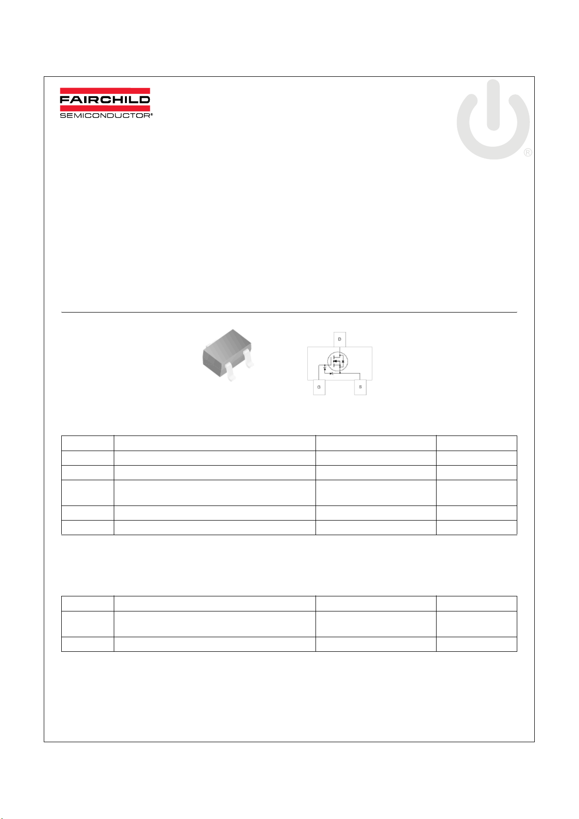
D
BSS138K — N-Channel Logic Level Enhancement Mode Field Effect Transistor
S
G
SOT - 23
Marking : SK
Absolute Maximum Ratings * T
= 25°C unless otherwise noted
A
Symbol Parameter Value Units
V
DSS
V
GSS
I
D
T
T
STG
* These ratings are limiting values above which the serviceability of any semiconductor device maybe impaired.
Drain-Source Voltage 50 V
Gate-Source Voltage ±12 V
Drain Current Continuous
Pulsed
Operating Junction Temperature Range -55 to +150 °C
J
0.22
0.88
Storage Temperature Range -55 to +150 °C
A
Thermal Characteristics
Symbol Parameter Value Units
P
R
θJA
* Device mounted on FR-4 PCB, 1 inch x 0.85 inch x 0.062 inch. Minimum land pad size
Total Device Dissipation
D
Derating above TA = 25°C
350
2.8
Thermal Resistance, Junction to Ambient * 350 °C/W
mW
mW/°C
© 2010 Fairchild Semiconductor Corporation www.fairchildsemi.com
BSS138K Rev. A2 1

BSS138K — N-Channel Logic Level Enhancement Mode Field Effect Transistor
Electrical Characteristics T
= 25°C unless otherwise noted
A
Symbol Parameter Test Condition Min. Typ. Max. Units
Off Characteristics
BV
BV
T
I
DSS
I
GSS
Drain-Source Breakdown Voltage VGS= 0V, ID=10µA50 V
DSS
Breakdown Voltage
DSS
Temperature Coefficient
J
I
=250µA, Referenced to 25°C0.11V/°C
D
Zero Gate Voltage Drain Current VDS= 50V, VGS= 0V 0.1 µA
Gate-Body Leakage VGS= ±12V, VDS= 0V
= ±10V, VDS= 0V
V
GS
VGS= ±5V, VDS= 0V
±1
±0.5
±0.05
On Characteristics
V
GS(th)
V
T
R
DS(ON)
I
D(ON)
g
GS(th)
FS
Gate Threshold Voltage VDS = VGS, ID = 250µA0.6 1.2V
Gate Threshold Voltage
Temperature Coefficient
J
Static Drain-Source
On-Resistance
= 1mA, Referenced to 25°C-1.4mV/°C
I
D
VGS = 1.8V, ID = 50mA,
VGS = 2.5V, ID = 50mA,
= 5V, ID = 50mA,
V
GS
2.5
2.0
1.6
On-State Drain Current VGS= 10V, VDS= 5V 0.2 A
Forward Transconductance VDS = 10V, ID = 200mA 200 mS
Dynamic Characteristics
C
C
oss
C
R
Input Capacitance
iss
Output Capacitance 9.75 pF
Reverse Transfer Capacitance 5.2
rss
Gate Resistance VDS= 5V, VGS= 10mV 281 Ω
G
= 25V, VGS= 0V, f = 1.0MHz
V
DS
58
Switching Characteristics
t
D(ON)
t
t
D(OFF)
t
Q
Q
Turn-On Delay Time
Turn-On Rise Time 5
r
Turn-Off Delay Time 60
Turn-Off Fall Time 35
f
Total Gate Change
g
Gate-Source Change 0.5
gs
Gate-Drain Change 0.5
gd
VDD = 30V, ID = 0.29A,
V
= 10V, R
GS
V
= 25V, ID = 0.2A,
DS
V
= 10V, IG = 0.1mA
GS
GEN
= 6Ω
5
2.4
Drain-Source Diode Characteristics and Maximum Ratings
V
Drain-Source Diode
sd
Forward Voltage
V
= 0V, IS = 115mA 1.2 V
GS
µA
Ω
ns
nCQ
© 2010 Fairchild Semiconductor Corporation www.fairchildsemi.com
BSS138K Rev. A2 2
 Loading...